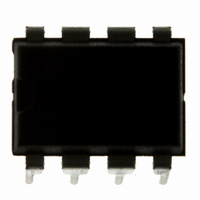
MC9S08QG4MPAE Freescale Semiconductor, MC9S08QG4MPAE Datasheet - Page 103

MC9S08QG4MPAE
Manufacturer Part Number
MC9S08QG4MPAE
Description
IC MCU 4K FLASH 8-PDIP
Manufacturer
Freescale Semiconductor
Series
HCS08r
Datasheet
1.MC9S08QG8CDTER.pdf
(314 pages)
Specifications of MC9S08QG4MPAE
Core Processor
HCS08
Core Size
8-Bit
Speed
20MHz
Connectivity
I²C, SCI, SPI
Peripherals
LVD, POR, PWM, WDT
Number Of I /o
4
Program Memory Size
4KB (4K x 8)
Program Memory Type
FLASH
Ram Size
256 x 8
Voltage - Supply (vcc/vdd)
1.8 V ~ 3.6 V
Data Converters
A/D 4x10b
Oscillator Type
Internal
Operating Temperature
-40°C ~ 125°C
Package / Case
8-DIP (0.300", 7.62mm)
Controller Family/series
HCS08
No. Of I/o's
6
Ram Memory Size
256Byte
Cpu Speed
20MHz
No. Of Timers
2
Embedded Interface Type
I2C, SCI, SPI
Rohs Compliant
Yes
Processor Series
S08QG
Core
HCS08
Data Bus Width
8 bit
Data Ram Size
256 B
Interface Type
I2C, SCI, SPI
Maximum Clock Frequency
20 MHz
Number Of Programmable I/os
12
Number Of Timers
1
Maximum Operating Temperature
+ 125 C
Mounting Style
Through Hole
3rd Party Development Tools
EWS08
Development Tools By Supplier
DEMO9S08QG8E
Minimum Operating Temperature
- 40 C
On-chip Adc
10 bit, 8 Channel
Lead Free Status / RoHS Status
Lead free / RoHS Compliant
Eeprom Size
-
Lead Free Status / Rohs Status
Details
- Current page: 103 of 314
- Download datasheet (6Mb)
Freescale Semiconductor
MOV opr8a,opr8a
MOV opr8a,X+
MOV #opr8i,opr8a
MOV ,X+,opr8a
MUL
NEG opr8a
NEGA
NEGX
NEG oprx8,X
NEG ,X
NEG oprx8,SP
NOP
NSA
ORA #opr8i
ORA opr8a
ORA opr16a
ORA oprx16,X
ORA oprx8,X
ORA ,X
ORA oprx16,SP
ORA oprx8,SP
PSHA
PSHH
PSHX
PULA
PULH
PULX
ROL opr8a
ROLA
ROLX
ROL oprx8,X
ROL ,X
ROL oprx8,SP
ROR opr8a
RORA
RORX
ROR oprx8,X
ROR ,X
ROR oprx8,SP
Source
Form
Move
(M)
In IX+/DIR and DIR/IX+ Modes,
H:X ← (H:X) + $0001
Unsigned multiply
X:A ← (X) × (A)
Negate
(Two’s Complement) A ← – (A) = $00 – (A)
No Operation — Uses 1 Bus Cycle
Nibble Swap Accumulator
A ← (A[3:0]:A[7:4])
Inclusive OR Accumulator and Memory
A ← (A) | (M)
Push Accumulator onto Stack
Push (A); SP ← (SP) – $0001
Push H (Index Register High) onto Stack
Push (H); SP ← (SP) – $0001
Push X (Index Register Low) onto Stack
Push (X); SP ← (SP) – $0001
Pull Accumulator from Stack
SP ← (SP + $0001); Pull (A)
Pull H (Index Register High) from Stack
SP ← (SP + $0001); Pull (H)
Pull X (Index Register Low) from Stack
SP ← (SP + $0001); Pull (X)
Rotate Left through Carry
Rotate Right through Carry
destination
C
b7
b7
Table 7-2. . Instruction Set Summary (Sheet 6 of 9)
← (M)
MC9S08QG8 and MC9S08QG4 Data Sheet, Rev. 5
Operation
source
b0
M ← – (M) = $00 – (M)
X ← – (X) = $00 – (X)
M ← – (M) = $00 – (M)
M ← – (M) = $00 – (M)
M ← – (M) = $00 – (M)
b0
C
DIR/DIR
DIR/IX+
IMM/DIR
IX+/DIR
INH
DIR
INH
INH
IX1
IX
SP1
INH
INH
IMM
DIR
EXT
IX2
IX1
IX
SP2
SP1
INH
INH
INH
INH
INH
INH
DIR
INH
INH
IX1
IX
SP1
DIR
INH
INH
IX1
IX
SP1
Object Code
9E 60
9E DA
9E EA
9E 69
9E 66
4E
5E
6E
7E
42
30
40
50
60
70
9D
62
AA
BA
CA
DA
EA
FA
87
8B
89
86
8A
88
39
49
59
69
79
36
46
56
66
76
dd dd
dd
ii dd
dd
dd
ff
ff
ii
dd
hh ll
ee ff
ff
ee ff
ff
dd
ff
ff
dd
ff
ff
Chapter 7 Central Processor Unit (S08CPUV2)
5
5
4
5
5
5
1
1
5
4
6
1
1
2
3
4
4
3
3
5
4
2
2
2
3
3
3
5
1
1
5
4
6
5
1
1
5
4
6
rpwpp
rfwpp
pwpp
rfwpp
ffffp
rfwpp
p
p
rfwpp
rfwp
prfwpp
p
p
pp
rpp
prpp
prpp
rpp
rfp
pprpp
prpp
sp
sp
sp
ufp
ufp
ufp
rfwpp
p
p
rfwpp
rfwp
prfwpp
rfwpp
p
p
rfwpp
rfwp
prfwpp
Cyc-by-Cyc
Details
VH I N Z C
0 – –
– 0 – – – 0
– – – – – –
– – – – – –
0 – –
– – – – – –
– – – – – –
– – – – – –
– – – – – –
– – – – – –
– – – – – –
on CCR
–
–
–
Affect
–
–
–
–
–
101
Related parts for MC9S08QG4MPAE
Image
Part Number
Description
Manufacturer
Datasheet
Request
R
Part Number:
Description:
Manufacturer:
Freescale Semiconductor, Inc
Datasheet:
Part Number:
Description:
Manufacturer:
Freescale Semiconductor, Inc
Datasheet:
Part Number:
Description:
Manufacturer:
Freescale Semiconductor, Inc
Datasheet:
Part Number:
Description:
Manufacturer:
Freescale Semiconductor, Inc
Datasheet:
Part Number:
Description:
Manufacturer:
Freescale Semiconductor, Inc
Datasheet:
Part Number:
Description:
Manufacturer:
Freescale Semiconductor, Inc
Datasheet:
Part Number:
Description:
Manufacturer:
Freescale Semiconductor, Inc
Datasheet:
Part Number:
Description:
Manufacturer:
Freescale Semiconductor, Inc
Datasheet:
Part Number:
Description:
Manufacturer:
Freescale Semiconductor, Inc
Datasheet:
Part Number:
Description:
Manufacturer:
Freescale Semiconductor, Inc
Datasheet:
Part Number:
Description:
Manufacturer:
Freescale Semiconductor, Inc
Datasheet:
Part Number:
Description:
Manufacturer:
Freescale Semiconductor, Inc
Datasheet:
Part Number:
Description:
Manufacturer:
Freescale Semiconductor, Inc
Datasheet:
Part Number:
Description:
Manufacturer:
Freescale Semiconductor, Inc
Datasheet:
Part Number:
Description:
Manufacturer:
Freescale Semiconductor, Inc
Datasheet:


