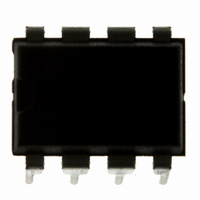
MC9S08QG4MPAE Freescale Semiconductor, MC9S08QG4MPAE Datasheet - Page 85

MC9S08QG4MPAE
Manufacturer Part Number
MC9S08QG4MPAE
Description
IC MCU 4K FLASH 8-PDIP
Manufacturer
Freescale Semiconductor
Series
HCS08r
Datasheet
1.MC9S08QG8CDTER.pdf
(314 pages)
Specifications of MC9S08QG4MPAE
Core Processor
HCS08
Core Size
8-Bit
Speed
20MHz
Connectivity
I²C, SCI, SPI
Peripherals
LVD, POR, PWM, WDT
Number Of I /o
4
Program Memory Size
4KB (4K x 8)
Program Memory Type
FLASH
Ram Size
256 x 8
Voltage - Supply (vcc/vdd)
1.8 V ~ 3.6 V
Data Converters
A/D 4x10b
Oscillator Type
Internal
Operating Temperature
-40°C ~ 125°C
Package / Case
8-DIP (0.300", 7.62mm)
Controller Family/series
HCS08
No. Of I/o's
6
Ram Memory Size
256Byte
Cpu Speed
20MHz
No. Of Timers
2
Embedded Interface Type
I2C, SCI, SPI
Rohs Compliant
Yes
Processor Series
S08QG
Core
HCS08
Data Bus Width
8 bit
Data Ram Size
256 B
Interface Type
I2C, SCI, SPI
Maximum Clock Frequency
20 MHz
Number Of Programmable I/os
12
Number Of Timers
1
Maximum Operating Temperature
+ 125 C
Mounting Style
Through Hole
3rd Party Development Tools
EWS08
Development Tools By Supplier
DEMO9S08QG8E
Minimum Operating Temperature
- 40 C
On-chip Adc
10 bit, 8 Channel
Lead Free Status / RoHS Status
Lead free / RoHS Compliant
Eeprom Size
-
Lead Free Status / Rohs Status
Details
- Current page: 85 of 314
- Download datasheet (6Mb)
6.4.3
This section provides information about the registers associated with the parallel I/O ports.
Refer to tables in
for all parallel I/O. This section refers to registers and control bits only by their names. A Freescale
Semiconductor-provided equate or header file normally is used to translate these names into the
appropriate absolute addresses.
6.4.3.1
6.4.3.2
Freescale Semiconductor
PTBDD[7:0]
PTBD[7:0]
Reset:
Reset:
Field
Field
7:0
7:0
W
W
R
R
PTBDD7
PTBD7
Port B Registers
Port B Data Register Bits — For port B pins that are inputs, reads return the logic level on the pin. For port B
pins that are configured as outputs, reads return the last value written to this register.
Writes are latched into all bits of this register. For port B pins that are configured as outputs, the logic level is
driven out the corresponding MCU pin.
Reset forces PTBD to all 0s, but these 0s are not driven out the corresponding pins because reset also configures
all port pins as high-impedance inputs with pullups disabled.
Data Direction for Port B Bits — These read/write bits control the direction of port B pins and what is read for
PTBD reads.
0 Input (output driver disabled) and reads return the pin value.
1 Output driver enabled for port B bit n and PTBD reads return the contents of PTBDn.
Port B Data (PTBD)
0
Port B Data Direction (PTBDD)
0
7
7
Chapter 4, “Memory Map and Register
PTBDD6
PTBD6
0
0
6
6
Figure 6-11. Data Direction for Port B (PTBDD)
Table 6-7. PTBDD Register Field Descriptions
MC9S08QG8 and MC9S08QG4 Data Sheet, Rev. 5
Table 6-6. PTBD Register Field Descriptions
Figure 6-10. Port B Data Register (PTBD)
PTBDD5
PTBD5
0
0
5
5
PTBDD4
PTBD4
0
0
4
4
Description
Description
Definition,” for the absolute address assignments
PTBDD3
PTBD3
3
0
3
0
PTBDD2
PTBD2
Chapter 6 Parallel Input/Output Control
0
0
2
2
PTBDD1
PTBD1
0
0
1
1
PTBDD0
PTBD0
0
0
0
0
83
Related parts for MC9S08QG4MPAE
Image
Part Number
Description
Manufacturer
Datasheet
Request
R
Part Number:
Description:
Manufacturer:
Freescale Semiconductor, Inc
Datasheet:
Part Number:
Description:
Manufacturer:
Freescale Semiconductor, Inc
Datasheet:
Part Number:
Description:
Manufacturer:
Freescale Semiconductor, Inc
Datasheet:
Part Number:
Description:
Manufacturer:
Freescale Semiconductor, Inc
Datasheet:
Part Number:
Description:
Manufacturer:
Freescale Semiconductor, Inc
Datasheet:
Part Number:
Description:
Manufacturer:
Freescale Semiconductor, Inc
Datasheet:
Part Number:
Description:
Manufacturer:
Freescale Semiconductor, Inc
Datasheet:
Part Number:
Description:
Manufacturer:
Freescale Semiconductor, Inc
Datasheet:
Part Number:
Description:
Manufacturer:
Freescale Semiconductor, Inc
Datasheet:
Part Number:
Description:
Manufacturer:
Freescale Semiconductor, Inc
Datasheet:
Part Number:
Description:
Manufacturer:
Freescale Semiconductor, Inc
Datasheet:
Part Number:
Description:
Manufacturer:
Freescale Semiconductor, Inc
Datasheet:
Part Number:
Description:
Manufacturer:
Freescale Semiconductor, Inc
Datasheet:
Part Number:
Description:
Manufacturer:
Freescale Semiconductor, Inc
Datasheet:
Part Number:
Description:
Manufacturer:
Freescale Semiconductor, Inc
Datasheet:


