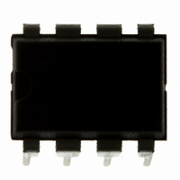
MC9S08QG4MPAE Freescale Semiconductor, MC9S08QG4MPAE Datasheet - Page 31

MC9S08QG4MPAE
Manufacturer Part Number
MC9S08QG4MPAE
Description
IC MCU 4K FLASH 8-PDIP
Manufacturer
Freescale Semiconductor
Series
HCS08r
Datasheet
1.MC9S08QG8CDTER.pdf
(314 pages)
Specifications of MC9S08QG4MPAE
Core Processor
HCS08
Core Size
8-Bit
Speed
20MHz
Connectivity
I²C, SCI, SPI
Peripherals
LVD, POR, PWM, WDT
Number Of I /o
4
Program Memory Size
4KB (4K x 8)
Program Memory Type
FLASH
Ram Size
256 x 8
Voltage - Supply (vcc/vdd)
1.8 V ~ 3.6 V
Data Converters
A/D 4x10b
Oscillator Type
Internal
Operating Temperature
-40°C ~ 125°C
Package / Case
8-DIP (0.300", 7.62mm)
Controller Family/series
HCS08
No. Of I/o's
6
Ram Memory Size
256Byte
Cpu Speed
20MHz
No. Of Timers
2
Embedded Interface Type
I2C, SCI, SPI
Rohs Compliant
Yes
Processor Series
S08QG
Core
HCS08
Data Bus Width
8 bit
Data Ram Size
256 B
Interface Type
I2C, SCI, SPI
Maximum Clock Frequency
20 MHz
Number Of Programmable I/os
12
Number Of Timers
1
Maximum Operating Temperature
+ 125 C
Mounting Style
Through Hole
3rd Party Development Tools
EWS08
Development Tools By Supplier
DEMO9S08QG8E
Minimum Operating Temperature
- 40 C
On-chip Adc
10 bit, 8 Channel
Lead Free Status / RoHS Status
Lead free / RoHS Compliant
Eeprom Size
-
Lead Free Status / Rohs Status
Details
- Current page: 31 of 314
- Download datasheet (6Mb)
2.2.5.1
To select drive strength or enable slew rate control or pullup devices, the user writes to the appropriate pin
control register located in the high page register block of the memory map. The pin control registers
operate independently of the parallel I/O registers and allow control of a port on an individual pin basis.
2.2.5.1.1
An internal pullup device can be enabled for each port pin by setting the corresponding bit in one of the
pullup enable registers (PTxPEn). The pullup device is disabled if the pin is configured as an output by the
parallel I/O control logic or any shared peripheral function, regardless of the state of the corresponding
pullup enable register bit. The pullup device is also disabled if the pin is controlled by an analog function.
The KBI module, when enabled for rising edge detection, causes an enabled internal pull device to be
configured as a pulldown.
2.2.5.2
Slew rate control can be enabled for each port pin by setting the corresponding bit in one of the slew rate
control registers (PTxSEn). When enabled, slew control limits the rate at which an output can transition in
order to reduce EMC emissions. Slew rate control has no effect on pins that are configured as inputs.
2.2.5.3
An output pin can be selected to have high output drive strength by setting the corresponding bit in one of
the drive strength select registers (PTxDSn). When high drive is selected, a pin is capable of sourcing and
sinking greater current. Even though every I/O pin can be selected as high drive, the user must ensure that
the total current source and sink limits for the chip are not exceeded. Drive strength selection is intended
to affect the DC behavior of I/O pins. However, the AC behavior is also affected. High drive allows a pin
to drive a greater load with the same switching speed as a low drive enabled pin into a smaller load.
Because of this, the EMC emissions may be affected by enabling pins as high drive.
Freescale Semiconductor
Pin Control Registers
Output Slew Rate Control
Output Drive Strength Select
To avoid extra current drain from floating input pins, the reset initialization
routine in the application program must either enable on-chip pullup devices
or change the direction of unused pins to outputs so the pins do not float.
When using the 8-pin devices, the user must either enable on-chip pullup
devices or change the direction of non-bonded out port B pins to outputs so
the pins do not float.
Internal Pullup Enable
MC9S08QG8 and MC9S08QG4 Data Sheet, Rev. 5
NOTE
Chapter 2 External Signal Description
29
Related parts for MC9S08QG4MPAE
Image
Part Number
Description
Manufacturer
Datasheet
Request
R
Part Number:
Description:
Manufacturer:
Freescale Semiconductor, Inc
Datasheet:
Part Number:
Description:
Manufacturer:
Freescale Semiconductor, Inc
Datasheet:
Part Number:
Description:
Manufacturer:
Freescale Semiconductor, Inc
Datasheet:
Part Number:
Description:
Manufacturer:
Freescale Semiconductor, Inc
Datasheet:
Part Number:
Description:
Manufacturer:
Freescale Semiconductor, Inc
Datasheet:
Part Number:
Description:
Manufacturer:
Freescale Semiconductor, Inc
Datasheet:
Part Number:
Description:
Manufacturer:
Freescale Semiconductor, Inc
Datasheet:
Part Number:
Description:
Manufacturer:
Freescale Semiconductor, Inc
Datasheet:
Part Number:
Description:
Manufacturer:
Freescale Semiconductor, Inc
Datasheet:
Part Number:
Description:
Manufacturer:
Freescale Semiconductor, Inc
Datasheet:
Part Number:
Description:
Manufacturer:
Freescale Semiconductor, Inc
Datasheet:
Part Number:
Description:
Manufacturer:
Freescale Semiconductor, Inc
Datasheet:
Part Number:
Description:
Manufacturer:
Freescale Semiconductor, Inc
Datasheet:
Part Number:
Description:
Manufacturer:
Freescale Semiconductor, Inc
Datasheet:
Part Number:
Description:
Manufacturer:
Freescale Semiconductor, Inc
Datasheet:


