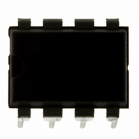
MC9S08QG4MPAE Freescale Semiconductor, MC9S08QG4MPAE Datasheet - Page 169

MC9S08QG4MPAE
Manufacturer Part Number
MC9S08QG4MPAE
Description
IC MCU 4K FLASH 8-PDIP
Manufacturer
Freescale Semiconductor
Series
HCS08r
Datasheet
1.MC9S08QG8CDTER.pdf
(314 pages)
Specifications of MC9S08QG4MPAE
Core Processor
HCS08
Core Size
8-Bit
Speed
20MHz
Connectivity
I²C, SCI, SPI
Peripherals
LVD, POR, PWM, WDT
Number Of I /o
4
Program Memory Size
4KB (4K x 8)
Program Memory Type
FLASH
Ram Size
256 x 8
Voltage - Supply (vcc/vdd)
1.8 V ~ 3.6 V
Data Converters
A/D 4x10b
Oscillator Type
Internal
Operating Temperature
-40°C ~ 125°C
Package / Case
8-DIP (0.300", 7.62mm)
Controller Family/series
HCS08
No. Of I/o's
6
Ram Memory Size
256Byte
Cpu Speed
20MHz
No. Of Timers
2
Embedded Interface Type
I2C, SCI, SPI
Rohs Compliant
Yes
Processor Series
S08QG
Core
HCS08
Data Bus Width
8 bit
Data Ram Size
256 B
Interface Type
I2C, SCI, SPI
Maximum Clock Frequency
20 MHz
Number Of Programmable I/os
12
Number Of Timers
1
Maximum Operating Temperature
+ 125 C
Mounting Style
Through Hole
3rd Party Development Tools
EWS08
Development Tools By Supplier
DEMO9S08QG8E
Minimum Operating Temperature
- 40 C
On-chip Adc
10 bit, 8 Channel
Lead Free Status / RoHS Status
Lead free / RoHS Compliant
Eeprom Size
-
Lead Free Status / Rohs Status
Details
- Current page: 169 of 314
- Download datasheet (6Mb)
11.4.1.4
The master can terminate the communication by generating a STOP signal to free the bus. However, the
master may generate a START signal followed by a calling command without generating a STOP signal
first. This is called repeated START. A STOP signal is defined as a low-to-high transition of SDA while
SCL at logical 1 (see
The master can generate a STOP even if the slave has generated an acknowledge at which point the slave
must release the bus.
11.4.1.5
As shown in
a STOP signal to terminate the communication. This is used by the master to communicate with another
slave or with the same slave in different mode (transmit/receive mode) without releasing the bus.
11.4.1.6
The IIC bus is a true multi-master bus that allows more than one master to be connected on it. If two or
more masters try to control the bus at the same time, a clock synchronization procedure determines the bus
clock, for which the low period is equal to the longest clock low period and the high is equal to the shortest
one among the masters. The relative priority of the contending masters is determined by a data arbitration
procedure, a bus master loses arbitration if it transmits logic 1 while another master transmits logic 0. The
losing masters immediately switch over to slave receive mode and stop driving SDA output. In this case,
the transition from master to slave mode does not generate a STOP condition. Meanwhile, a status bit is
set by hardware to indicate loss of arbitration.
11.4.1.7
Because wire-AND logic is performed on the SCL line, a high-to-low transition on the SCL line affects all
the devices connected on the bus. The devices start counting their low period and after a device’s clock has
gone low, it holds the SCL line low until the clock high state is reached. However, the change of low to
high in this device clock may not change the state of the SCL line if another device clock is still within its
low period. Therefore, synchronized clock SCL is held low by the device with the longest low period.
Devices with shorter low periods enter a high wait state during this time (see
devices concerned have counted off their low period, the synchronized clock SCL line is released and
pulled high. There is then no difference between the device clocks and the state of the SCL line and all the
devices start counting their high periods. The first device to complete its high period pulls the SCL line
low again.
Freescale Semiconductor
Figure
STOP Signal
Repeated START Signal
Arbitration Procedure
Clock Synchronization
11-8, a repeated START signal is a START signal generated without first generating
Figure
11-8).
MC9S08QG8 and MC9S08QG4 Data Sheet, Rev. 5
Figure
Inter-Integrated Circuit (S08IICV1)
11-9). When all
167
Related parts for MC9S08QG4MPAE
Image
Part Number
Description
Manufacturer
Datasheet
Request
R
Part Number:
Description:
Manufacturer:
Freescale Semiconductor, Inc
Datasheet:
Part Number:
Description:
Manufacturer:
Freescale Semiconductor, Inc
Datasheet:
Part Number:
Description:
Manufacturer:
Freescale Semiconductor, Inc
Datasheet:
Part Number:
Description:
Manufacturer:
Freescale Semiconductor, Inc
Datasheet:
Part Number:
Description:
Manufacturer:
Freescale Semiconductor, Inc
Datasheet:
Part Number:
Description:
Manufacturer:
Freescale Semiconductor, Inc
Datasheet:
Part Number:
Description:
Manufacturer:
Freescale Semiconductor, Inc
Datasheet:
Part Number:
Description:
Manufacturer:
Freescale Semiconductor, Inc
Datasheet:
Part Number:
Description:
Manufacturer:
Freescale Semiconductor, Inc
Datasheet:
Part Number:
Description:
Manufacturer:
Freescale Semiconductor, Inc
Datasheet:
Part Number:
Description:
Manufacturer:
Freescale Semiconductor, Inc
Datasheet:
Part Number:
Description:
Manufacturer:
Freescale Semiconductor, Inc
Datasheet:
Part Number:
Description:
Manufacturer:
Freescale Semiconductor, Inc
Datasheet:
Part Number:
Description:
Manufacturer:
Freescale Semiconductor, Inc
Datasheet:
Part Number:
Description:
Manufacturer:
Freescale Semiconductor, Inc
Datasheet:


