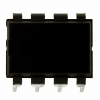
MC9S08QG4MPAE Freescale Semiconductor, MC9S08QG4MPAE Datasheet - Page 51

MC9S08QG4MPAE
Manufacturer Part Number
MC9S08QG4MPAE
Description
IC MCU 4K FLASH 8-PDIP
Manufacturer
Freescale Semiconductor
Series
HCS08r
Datasheet
1.MC9S08QG8CDTER.pdf
(314 pages)
Specifications of MC9S08QG4MPAE
Core Processor
HCS08
Core Size
8-Bit
Speed
20MHz
Connectivity
I²C, SCI, SPI
Peripherals
LVD, POR, PWM, WDT
Number Of I /o
4
Program Memory Size
4KB (4K x 8)
Program Memory Type
FLASH
Ram Size
256 x 8
Voltage - Supply (vcc/vdd)
1.8 V ~ 3.6 V
Data Converters
A/D 4x10b
Oscillator Type
Internal
Operating Temperature
-40°C ~ 125°C
Package / Case
8-DIP (0.300", 7.62mm)
Controller Family/series
HCS08
No. Of I/o's
6
Ram Memory Size
256Byte
Cpu Speed
20MHz
No. Of Timers
2
Embedded Interface Type
I2C, SCI, SPI
Rohs Compliant
Yes
Processor Series
S08QG
Core
HCS08
Data Bus Width
8 bit
Data Ram Size
256 B
Interface Type
I2C, SCI, SPI
Maximum Clock Frequency
20 MHz
Number Of Programmable I/os
12
Number Of Timers
1
Maximum Operating Temperature
+ 125 C
Mounting Style
Through Hole
3rd Party Development Tools
EWS08
Development Tools By Supplier
DEMO9S08QG8E
Minimum Operating Temperature
- 40 C
On-chip Adc
10 bit, 8 Channel
Lead Free Status / RoHS Status
Lead free / RoHS Compliant
Eeprom Size
-
Lead Free Status / Rohs Status
Details
- Current page: 51 of 314
- Download datasheet (6Mb)
4.5.4
The burst program command is used to program sequential bytes of data in less time than would be
required using the standard program command. This is possible because the high voltage to the FLASH
array does not need to be disabled between program operations. Ordinarily, when a program or erase
command is issued, an internal charge pump associated with the FLASH memory must be enabled to
supply high voltage to the array. Upon completion of the command, the charge pump is turned off. When
a burst program command is issued, the charge pump is enabled and then remains enabled after completion
of the burst program operation if these two conditions are met:
Freescale Semiconductor
•
•
The next burst program command has been queued before the current program operation has
completed.
The next sequential address selects a byte on the same physical row as the current byte being
programmed. A row of FLASH memory consists of 64 bytes. A byte within a row is selected by
addresses A5 through A0. A new row begins when addresses A5 through A0 are all zero.
Burst Program Execution
FLASH PROGRAM AND
ERASE FLOW
Figure 4-2. FLASH Program and Erase Flowchart
MC9S08QG8 and MC9S08QG4 Data Sheet, Rev. 5
0
TO BUFFER ADDRESS AND DATA
WRITE COMMAND TO FCMD
AND CLEAR FCBEF (Note 2)
WRITE TO FCDIV (Note 1)
TO LAUNCH COMMAND
WRITE 1 TO FCBEF
WRITE TO FLASH
CLEAR ERROR
FACCERR ?
FPVIOL OR
FACCERR ?
FCCF ?
START
DONE
1
NO
1
YES
0
Note 2: Wait at least four bus cycles
Note 1: Required only once after reset.
Chapter 4 Memory Map and Register Definition
ERROR EXIT
before checking FCBEF or FCCF.
49
Related parts for MC9S08QG4MPAE
Image
Part Number
Description
Manufacturer
Datasheet
Request
R
Part Number:
Description:
Manufacturer:
Freescale Semiconductor, Inc
Datasheet:
Part Number:
Description:
Manufacturer:
Freescale Semiconductor, Inc
Datasheet:
Part Number:
Description:
Manufacturer:
Freescale Semiconductor, Inc
Datasheet:
Part Number:
Description:
Manufacturer:
Freescale Semiconductor, Inc
Datasheet:
Part Number:
Description:
Manufacturer:
Freescale Semiconductor, Inc
Datasheet:
Part Number:
Description:
Manufacturer:
Freescale Semiconductor, Inc
Datasheet:
Part Number:
Description:
Manufacturer:
Freescale Semiconductor, Inc
Datasheet:
Part Number:
Description:
Manufacturer:
Freescale Semiconductor, Inc
Datasheet:
Part Number:
Description:
Manufacturer:
Freescale Semiconductor, Inc
Datasheet:
Part Number:
Description:
Manufacturer:
Freescale Semiconductor, Inc
Datasheet:
Part Number:
Description:
Manufacturer:
Freescale Semiconductor, Inc
Datasheet:
Part Number:
Description:
Manufacturer:
Freescale Semiconductor, Inc
Datasheet:
Part Number:
Description:
Manufacturer:
Freescale Semiconductor, Inc
Datasheet:
Part Number:
Description:
Manufacturer:
Freescale Semiconductor, Inc
Datasheet:
Part Number:
Description:
Manufacturer:
Freescale Semiconductor, Inc
Datasheet:


