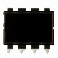
MC9S08QG4MPAE Freescale Semiconductor, MC9S08QG4MPAE Datasheet - Page 28

MC9S08QG4MPAE
Manufacturer Part Number
MC9S08QG4MPAE
Description
IC MCU 4K FLASH 8-PDIP
Manufacturer
Freescale Semiconductor
Series
HCS08r
Datasheet
1.MC9S08QG8CDTER.pdf
(314 pages)
Specifications of MC9S08QG4MPAE
Core Processor
HCS08
Core Size
8-Bit
Speed
20MHz
Connectivity
I²C, SCI, SPI
Peripherals
LVD, POR, PWM, WDT
Number Of I /o
4
Program Memory Size
4KB (4K x 8)
Program Memory Type
FLASH
Ram Size
256 x 8
Voltage - Supply (vcc/vdd)
1.8 V ~ 3.6 V
Data Converters
A/D 4x10b
Oscillator Type
Internal
Operating Temperature
-40°C ~ 125°C
Package / Case
8-DIP (0.300", 7.62mm)
Controller Family/series
HCS08
No. Of I/o's
6
Ram Memory Size
256Byte
Cpu Speed
20MHz
No. Of Timers
2
Embedded Interface Type
I2C, SCI, SPI
Rohs Compliant
Yes
Processor Series
S08QG
Core
HCS08
Data Bus Width
8 bit
Data Ram Size
256 B
Interface Type
I2C, SCI, SPI
Maximum Clock Frequency
20 MHz
Number Of Programmable I/os
12
Number Of Timers
1
Maximum Operating Temperature
+ 125 C
Mounting Style
Through Hole
3rd Party Development Tools
EWS08
Development Tools By Supplier
DEMO9S08QG8E
Minimum Operating Temperature
- 40 C
On-chip Adc
10 bit, 8 Channel
Lead Free Status / RoHS Status
Lead free / RoHS Compliant
Eeprom Size
-
Lead Free Status / Rohs Status
Details
- Current page: 28 of 314
- Download datasheet (6Mb)
Chapter 2 External Signal Description
2.2.1
V
I/O buffer circuitry, ACMP and ADC modules, and to an internal voltage regulator. The internal voltage
regulator provides a regulated lower-voltage source to the CPU and other internal circuitry of the MCU.
Typically, application systems have two separate capacitors across the power pins: a bulk electrolytic
capacitor, such as a 10-μF tantalum capacitor, to provide bulk charge storage for the overall system, and a
bypass capacitor, such as a 0.1-μF ceramic capacitor, located as near to the MCU power pins as practical
to suppress high-frequency noise.
26
ASYNCHRONOUS
DD
INTERRUPT
V
INPUT
DD
and V
C1
NOTES:
SYSTEM
POWER
BACKGROUND HEADER
NOTE 1
1. Not required if using the internal clock option.
2. XTAL is the same pin as PTB6; EXTAL the same pin as PTB7.
3. The RESET pin can only be used to reset into user mode; you can not enter BDM using the RESET pin.
4. IRQ feature has optional internal pullup device.
5. RC filter on RESET/IRQ pin recommended for noisy environments.
SS
Power
BDM can be entered by holding MS low during POR or writing a 1 to BDFR in SBDFR with MS low after
issuing the BDM command.
+
3 V
X1
are the primary power supply pins for the MCU. This voltage source supplies power to all
OPTIONAL
R
MANUAL
C
RESET
10 μF
F
BLK
C2
V
+
DD
V
DD
R
4.7 kΩ–10 kΩ
S
0.1 μF
0.1 μF
C
MC9S08QG8 and MC9S08QG4 Data Sheet, Rev. 5
BY
Figure 2-4. Basic System Connections
V
V
XTAL
NOTE 2
NOTE 2
DD
SS
EXTAL
BKGD
RESET/IRQ
MC9S08QG8/4
PORT
PORT
B
A
PTB4/MISO
PTB6/SDA/XTAL
PTB2/KBIP6/SPSCK/ADP6
PTB5/TPMCH1/SS
PTB7/SCL/EXTAL
PTA0/KBIP0/TPMCH0/ADP0/ACMP+
PTA1/KBIP1/ADP1/ACMP–
PTA2/KBIP2/SDA/ADP2
PTA3/KBIP3/SCL/ADP3
PTA4/ACMPO/BKGD/MS
PTA5/IRQ/TCLK/RESET
PTB0/KBIP4/RxD/ADP4
PTB1/KBIP5/TxD/ADP5
PTB3/KBIP7/MOSI/ADP7
Freescale Semiconductor
INTERFACE TO
APPLICATION
PERIPHERAL
SYSTEM
I/O AND
Related parts for MC9S08QG4MPAE
Image
Part Number
Description
Manufacturer
Datasheet
Request
R
Part Number:
Description:
Manufacturer:
Freescale Semiconductor, Inc
Datasheet:
Part Number:
Description:
Manufacturer:
Freescale Semiconductor, Inc
Datasheet:
Part Number:
Description:
Manufacturer:
Freescale Semiconductor, Inc
Datasheet:
Part Number:
Description:
Manufacturer:
Freescale Semiconductor, Inc
Datasheet:
Part Number:
Description:
Manufacturer:
Freescale Semiconductor, Inc
Datasheet:
Part Number:
Description:
Manufacturer:
Freescale Semiconductor, Inc
Datasheet:
Part Number:
Description:
Manufacturer:
Freescale Semiconductor, Inc
Datasheet:
Part Number:
Description:
Manufacturer:
Freescale Semiconductor, Inc
Datasheet:
Part Number:
Description:
Manufacturer:
Freescale Semiconductor, Inc
Datasheet:
Part Number:
Description:
Manufacturer:
Freescale Semiconductor, Inc
Datasheet:
Part Number:
Description:
Manufacturer:
Freescale Semiconductor, Inc
Datasheet:
Part Number:
Description:
Manufacturer:
Freescale Semiconductor, Inc
Datasheet:
Part Number:
Description:
Manufacturer:
Freescale Semiconductor, Inc
Datasheet:
Part Number:
Description:
Manufacturer:
Freescale Semiconductor, Inc
Datasheet:
Part Number:
Description:
Manufacturer:
Freescale Semiconductor, Inc
Datasheet:


