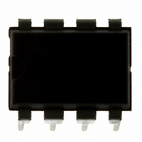
MC9S08QG4MPAE Freescale Semiconductor, MC9S08QG4MPAE Datasheet - Page 32

MC9S08QG4MPAE
Manufacturer Part Number
MC9S08QG4MPAE
Description
IC MCU 4K FLASH 8-PDIP
Manufacturer
Freescale Semiconductor
Series
HCS08r
Datasheet
1.MC9S08QG8CDTER.pdf
(314 pages)
Specifications of MC9S08QG4MPAE
Core Processor
HCS08
Core Size
8-Bit
Speed
20MHz
Connectivity
I²C, SCI, SPI
Peripherals
LVD, POR, PWM, WDT
Number Of I /o
4
Program Memory Size
4KB (4K x 8)
Program Memory Type
FLASH
Ram Size
256 x 8
Voltage - Supply (vcc/vdd)
1.8 V ~ 3.6 V
Data Converters
A/D 4x10b
Oscillator Type
Internal
Operating Temperature
-40°C ~ 125°C
Package / Case
8-DIP (0.300", 7.62mm)
Controller Family/series
HCS08
No. Of I/o's
6
Ram Memory Size
256Byte
Cpu Speed
20MHz
No. Of Timers
2
Embedded Interface Type
I2C, SCI, SPI
Rohs Compliant
Yes
Processor Series
S08QG
Core
HCS08
Data Bus Width
8 bit
Data Ram Size
256 B
Interface Type
I2C, SCI, SPI
Maximum Clock Frequency
20 MHz
Number Of Programmable I/os
12
Number Of Timers
1
Maximum Operating Temperature
+ 125 C
Mounting Style
Through Hole
3rd Party Development Tools
EWS08
Development Tools By Supplier
DEMO9S08QG8E
Minimum Operating Temperature
- 40 C
On-chip Adc
10 bit, 8 Channel
Lead Free Status / RoHS Status
Lead free / RoHS Compliant
Eeprom Size
-
Lead Free Status / Rohs Status
Details
- Current page: 32 of 314
- Download datasheet (6Mb)
Chapter 2 External Signal Description
30
Port Pins
Analog comparator
Serial peripheral interface
Keyboard interrupts
Timer/PWM
Inter-integrated circuit
Serial communications interface
Oscillator/clocking
Analog-to-digital
Power/core
Reset and interrupts
Signal Function
1
2
3
24-pin 16-pin
Pin does not contain a clamp diode to V
voltage measured on the internally pulled-up RESET pin will not be pulled to V
internal gates connected to this pin are pulled to V
IIC pins can be repositioned using IICPS in SOPT2; default reset locations are on PTA2
and PTA3.
If ACMP and ADC are both enabled, both will have access to the pin.
24
10
12
13
14
15
16
17
18
20
1
2
3
4
5
6
Pin Number
10
11
12
13
14
15
16
2
3
4
5
6
7
1
8
9
PTAx, PTBx
ACMPO, ACMP–, ACMP+
SS, MISO, MOSI, SPSCK
KBIPx
TCLK, TPMCHx
SCL, SDA
TxD, RxD
EXTAL, XTAL
ADPx
BKGD/MS, V
RESET, IRQ
MC9S08QG8 and MC9S08QG4 Data Sheet, Rev. 5
8-pin
—
—
—
—
—
—
—
—
1
2
3
4
5
6
7
8
Table 2-2. Pin Function Reference
Example(s)
PTA5
PTA4
PTB7
PTB6
PTB5
PTB4
PTB3
PTB2
PTB1
PTB0
PTA3
PTA2
PTA1
PTA0
Table 2-1. Pin Sharing Priority
Port Pin
Lowest
DD
1
, V
SS
IRQ
KBIP7
KBIP6
KBIP5
KBIP4
KBIP3
KBIP2
KBIP1
KBIP0
DD
Alt 1
and should not be driven above V
Chapter 6, “Parallel Input/Output
Chapter 8, “Analog Comparator
Chapter 15, “Serial Peripheral Interface (S08SPIV3)
Chapter 12, “Keyboard Interrupt
Chapter 16, “Timer/Pulse-Width Modulator
Chapter 11, “Inter-Integrated Circuit
Chapter 14, “Serial Communications Interface (S08SCIV3)
Chapter 10, “Internal Clock Source
Chapter 9, “Analog-to-Digital Converter
Chapter 2, “External Signal
Chapter 5, “Resets, Interrupts, and General System
TCLK
ACMPO
SCL
SDA
TPMCH1
MISO
MOSI
SPSCK
TxD
RxD
SCL
SDA
TPMCH0
DD
Priority
Alt 2
.
2
2
2
2
BKGD
EXTAL
XTAL
SS
ADP7
ADP6
ADP5
ADP4
ADP3
ADP2
ADP1
ADP0
Alt 3
3
3
Reference
Description”
MS
V
V
ACMP–
ACMP+
Highest
DD
SS
(S08ACMPV2)”
RESET
DD
(S08KBIV2)”
Control”
Alt 4
DD
. The
(S08ICSV1)”
Freescale Semiconductor
. The
(S08IICV1)”
3
3
(S08ADC10V1)”
(S08TPMV2)”
Control”
Related parts for MC9S08QG4MPAE
Image
Part Number
Description
Manufacturer
Datasheet
Request
R
Part Number:
Description:
Manufacturer:
Freescale Semiconductor, Inc
Datasheet:
Part Number:
Description:
Manufacturer:
Freescale Semiconductor, Inc
Datasheet:
Part Number:
Description:
Manufacturer:
Freescale Semiconductor, Inc
Datasheet:
Part Number:
Description:
Manufacturer:
Freescale Semiconductor, Inc
Datasheet:
Part Number:
Description:
Manufacturer:
Freescale Semiconductor, Inc
Datasheet:
Part Number:
Description:
Manufacturer:
Freescale Semiconductor, Inc
Datasheet:
Part Number:
Description:
Manufacturer:
Freescale Semiconductor, Inc
Datasheet:
Part Number:
Description:
Manufacturer:
Freescale Semiconductor, Inc
Datasheet:
Part Number:
Description:
Manufacturer:
Freescale Semiconductor, Inc
Datasheet:
Part Number:
Description:
Manufacturer:
Freescale Semiconductor, Inc
Datasheet:
Part Number:
Description:
Manufacturer:
Freescale Semiconductor, Inc
Datasheet:
Part Number:
Description:
Manufacturer:
Freescale Semiconductor, Inc
Datasheet:
Part Number:
Description:
Manufacturer:
Freescale Semiconductor, Inc
Datasheet:
Part Number:
Description:
Manufacturer:
Freescale Semiconductor, Inc
Datasheet:
Part Number:
Description:
Manufacturer:
Freescale Semiconductor, Inc
Datasheet:


