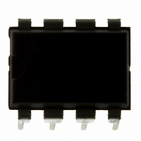
MC9S08QG4MPAE Freescale Semiconductor, MC9S08QG4MPAE Datasheet - Page 130

MC9S08QG4MPAE
Manufacturer Part Number
MC9S08QG4MPAE
Description
IC MCU 4K FLASH 8-PDIP
Manufacturer
Freescale Semiconductor
Series
HCS08r
Datasheet
1.MC9S08QG8CDTER.pdf
(314 pages)
Specifications of MC9S08QG4MPAE
Core Processor
HCS08
Core Size
8-Bit
Speed
20MHz
Connectivity
I²C, SCI, SPI
Peripherals
LVD, POR, PWM, WDT
Number Of I /o
4
Program Memory Size
4KB (4K x 8)
Program Memory Type
FLASH
Ram Size
256 x 8
Voltage - Supply (vcc/vdd)
1.8 V ~ 3.6 V
Data Converters
A/D 4x10b
Oscillator Type
Internal
Operating Temperature
-40°C ~ 125°C
Package / Case
8-DIP (0.300", 7.62mm)
Controller Family/series
HCS08
No. Of I/o's
6
Ram Memory Size
256Byte
Cpu Speed
20MHz
No. Of Timers
2
Embedded Interface Type
I2C, SCI, SPI
Rohs Compliant
Yes
Processor Series
S08QG
Core
HCS08
Data Bus Width
8 bit
Data Ram Size
256 B
Interface Type
I2C, SCI, SPI
Maximum Clock Frequency
20 MHz
Number Of Programmable I/os
12
Number Of Timers
1
Maximum Operating Temperature
+ 125 C
Mounting Style
Through Hole
3rd Party Development Tools
EWS08
Development Tools By Supplier
DEMO9S08QG8E
Minimum Operating Temperature
- 40 C
On-chip Adc
10 bit, 8 Channel
Lead Free Status / RoHS Status
Lead free / RoHS Compliant
Eeprom Size
-
Lead Free Status / Rohs Status
Details
- Current page: 130 of 314
- Download datasheet (6Mb)
Analog-to-Digital Converter (S08ADC10V1)
9.3.9
APCTL2 is used to control channels 8–15 of the ADC module.
128
ADPC15
ADPC14
ADPC13
ADPC12
ADPC11
ADPC10
ADPC1
ADPC0
Field
Field
7
6
5
4
3
2
1
0
Reset:
W
ADC Pin Control 15 — ADPC15 is used to control the pin associated with channel AD15.
0 AD15 pin I/O control enabled
1 AD15 pin I/O control disabled
ADC Pin Control 14 — ADPC14 is used to control the pin associated with channel AD14.
0 AD14 pin I/O control enabled
1 AD14 pin I/O control disabled
ADC Pin Control 13 — ADPC13 is used to control the pin associated with channel AD13.
0 AD13 pin I/O control enabled
1 AD13 pin I/O control disabled
ADC Pin Control 12 — ADPC12 is used to control the pin associated with channel AD12.
0 AD12 pin I/O control enabled
1 AD12 pin I/O control disabled
ADC Pin Control 11 — ADPC11 is used to control the pin associated with channel AD11.
0 AD11 pin I/O control enabled
1 AD11 pin I/O control disabled
ADC Pin Control 10 — ADPC10 is used to control the pin associated with channel AD10.
0 AD10 pin I/O control enabled
1 AD10 pin I/O control disabled
R
Pin Control 2 Register (APCTL2)
ADC Pin Control 1 — ADPC1 is used to control the pin associated with channel AD1.
0 AD1 pin I/O control enabled
1 AD1 pin I/O control disabled
ADC Pin Control 0 — ADPC0 is used to control the pin associated with channel AD0.
0 AD0 pin I/O control enabled
1 AD0 pin I/O control disabled
ADPC15
7
0
Table 9-9. APCTL1 Register Field Descriptions (continued)
ADPC14
0
Table 9-10. APCTL2 Register Field Descriptions
6
Figure 9-12. Pin Control 2 Register (APCTL2)
MC9S08QG8 and MC9S08QG4 Data Sheet, Rev. 5
ADPC13
0
5
ADPC12
0
4
Description
Description
ADPC11
0
3
ADPC10
0
2
ADPC9
Freescale Semiconductor
0
1
ADPC8
0
0
Related parts for MC9S08QG4MPAE
Image
Part Number
Description
Manufacturer
Datasheet
Request
R
Part Number:
Description:
Manufacturer:
Freescale Semiconductor, Inc
Datasheet:
Part Number:
Description:
Manufacturer:
Freescale Semiconductor, Inc
Datasheet:
Part Number:
Description:
Manufacturer:
Freescale Semiconductor, Inc
Datasheet:
Part Number:
Description:
Manufacturer:
Freescale Semiconductor, Inc
Datasheet:
Part Number:
Description:
Manufacturer:
Freescale Semiconductor, Inc
Datasheet:
Part Number:
Description:
Manufacturer:
Freescale Semiconductor, Inc
Datasheet:
Part Number:
Description:
Manufacturer:
Freescale Semiconductor, Inc
Datasheet:
Part Number:
Description:
Manufacturer:
Freescale Semiconductor, Inc
Datasheet:
Part Number:
Description:
Manufacturer:
Freescale Semiconductor, Inc
Datasheet:
Part Number:
Description:
Manufacturer:
Freescale Semiconductor, Inc
Datasheet:
Part Number:
Description:
Manufacturer:
Freescale Semiconductor, Inc
Datasheet:
Part Number:
Description:
Manufacturer:
Freescale Semiconductor, Inc
Datasheet:
Part Number:
Description:
Manufacturer:
Freescale Semiconductor, Inc
Datasheet:
Part Number:
Description:
Manufacturer:
Freescale Semiconductor, Inc
Datasheet:
Part Number:
Description:
Manufacturer:
Freescale Semiconductor, Inc
Datasheet:


