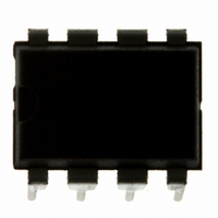
MC9S08QG4MPAE Freescale Semiconductor, MC9S08QG4MPAE Datasheet - Page 272

MC9S08QG4MPAE
Manufacturer Part Number
MC9S08QG4MPAE
Description
IC MCU 4K FLASH 8-PDIP
Manufacturer
Freescale Semiconductor
Series
HCS08r
Datasheet
1.MC9S08QG8CDTER.pdf
(314 pages)
Specifications of MC9S08QG4MPAE
Core Processor
HCS08
Core Size
8-Bit
Speed
20MHz
Connectivity
I²C, SCI, SPI
Peripherals
LVD, POR, PWM, WDT
Number Of I /o
4
Program Memory Size
4KB (4K x 8)
Program Memory Type
FLASH
Ram Size
256 x 8
Voltage - Supply (vcc/vdd)
1.8 V ~ 3.6 V
Data Converters
A/D 4x10b
Oscillator Type
Internal
Operating Temperature
-40°C ~ 125°C
Package / Case
8-DIP (0.300", 7.62mm)
Controller Family/series
HCS08
No. Of I/o's
6
Ram Memory Size
256Byte
Cpu Speed
20MHz
No. Of Timers
2
Embedded Interface Type
I2C, SCI, SPI
Rohs Compliant
Yes
Processor Series
S08QG
Core
HCS08
Data Bus Width
8 bit
Data Ram Size
256 B
Interface Type
I2C, SCI, SPI
Maximum Clock Frequency
20 MHz
Number Of Programmable I/os
12
Number Of Timers
1
Maximum Operating Temperature
+ 125 C
Mounting Style
Through Hole
3rd Party Development Tools
EWS08
Development Tools By Supplier
DEMO9S08QG8E
Minimum Operating Temperature
- 40 C
On-chip Adc
10 bit, 8 Channel
Lead Free Status / RoHS Status
Lead free / RoHS Compliant
Eeprom Size
-
Lead Free Status / Rohs Status
Details
- Current page: 272 of 314
- Download datasheet (6Mb)
1
2
3
4
5
6
7
Appendix A Electrical Characteristics
270
Internal pulldown resistor (KBI)
Output high voltage — low drive (PTxDSn = 0)
Output high voltage — high drive (PTxDSn = 1)
Maximum total I
Output low voltage — low drive (PTxDSn = 0)
Output low voltage — high drive (PTxDSn = 1)
Maximum total I
DC injection current
Input capacitance (all non-supply pins)
RAM will retain data down to POR voltage. RAM data not guaranteed to be valid following a POR.
This parameter is characterized and not tested on each device.
Measurement condition for pull resistors: V
PTA5/IRQ/TCLK/RESET pullup resistor may not pullup to the specified minimum V
to guarantee that a logic 1 will be read on any port input when the pullup is enabled and no DC load is present on the pin.
All functional non-supply pins are internally clamped to V
Input must be current limited to the value specified. To determine the value of the required current-limiting resistor, calculate
resistance values for positive and negative clamp voltages, then use the larger of the two values.
Power supply must maintain regulation within operating V
conditions. If positive injection current (V
in external power supply going out of regulation. Ensure external V
current. This will be the greatest risk when the MCU is not consuming power. Examples are: if no system clock is present, or if
clock rate is very low (which would reduce overall power consumption).
I
I
I
I
I
I
Single pin limit
Total MCU limit, includes sum of all stressed pins
I
OH
OH
OH
OL
OL
OL
I
OL
OH
V
= 2.0 mA (V
= 6 mA (V
= 3 mA (V
= 10.0 mA (V
= –10 mA (V
= –6 mA (V
= –3 mA (V
= –2 mA (V
IN
< V
SS
, V
OH
OL
DD
DD
DD
DD
DD
IN
DD
for all port pins
DD
for all port pins
≥ 2.3 V)
≥ 1.8 V)
DD
2, 5, 6, 7
> V
≥ 2.3 V)
≥ 1.8 V)
≥ 1.8 V)
≥ 1.8 V)
≥ 2.7 V)
≥ 2.7 V)
DD
Parameter
MC9S08QG8 and MC9S08QG4 Data Sheet, Rev. 5
Table A-6. DC Characteristics (continued)
In
> V
In
= V
DD
) is greater than I
SS
for pullup and V
SS
DD
and V
range during instantaneous and operating maximum current
Symbol
| I
DD
R
V
DD
V
I
OHT
C
OLT
I
DD
OH
OL
IC
, the injection current may flow out of V
PD
In
In
.
= V
load will shunt current greater than maximum injection
|
DD
for pulldown.
V
V
DD
DD
17.5
–0.2
Min
–5
—
—
—
—
—
—
—
IH
– 0.5
– 0.5
. However, all ports are functionally tested
Typical
Freescale Semiconductor
DD
Max
52.5
0.5
0.5
0.5
0.5
0.2
60
60
—
—
—
—
5
7
and could result
Unit
mA
mA
mA
mA
kΩ
pF
V
V
Related parts for MC9S08QG4MPAE
Image
Part Number
Description
Manufacturer
Datasheet
Request
R
Part Number:
Description:
Manufacturer:
Freescale Semiconductor, Inc
Datasheet:
Part Number:
Description:
Manufacturer:
Freescale Semiconductor, Inc
Datasheet:
Part Number:
Description:
Manufacturer:
Freescale Semiconductor, Inc
Datasheet:
Part Number:
Description:
Manufacturer:
Freescale Semiconductor, Inc
Datasheet:
Part Number:
Description:
Manufacturer:
Freescale Semiconductor, Inc
Datasheet:
Part Number:
Description:
Manufacturer:
Freescale Semiconductor, Inc
Datasheet:
Part Number:
Description:
Manufacturer:
Freescale Semiconductor, Inc
Datasheet:
Part Number:
Description:
Manufacturer:
Freescale Semiconductor, Inc
Datasheet:
Part Number:
Description:
Manufacturer:
Freescale Semiconductor, Inc
Datasheet:
Part Number:
Description:
Manufacturer:
Freescale Semiconductor, Inc
Datasheet:
Part Number:
Description:
Manufacturer:
Freescale Semiconductor, Inc
Datasheet:
Part Number:
Description:
Manufacturer:
Freescale Semiconductor, Inc
Datasheet:
Part Number:
Description:
Manufacturer:
Freescale Semiconductor, Inc
Datasheet:
Part Number:
Description:
Manufacturer:
Freescale Semiconductor, Inc
Datasheet:
Part Number:
Description:
Manufacturer:
Freescale Semiconductor, Inc
Datasheet:


