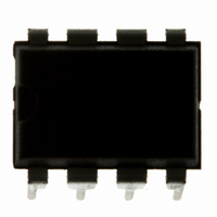
MC9S08QG4MPAE Freescale Semiconductor, MC9S08QG4MPAE Datasheet - Page 150

MC9S08QG4MPAE
Manufacturer Part Number
MC9S08QG4MPAE
Description
IC MCU 4K FLASH 8-PDIP
Manufacturer
Freescale Semiconductor
Series
HCS08r
Datasheet
1.MC9S08QG8CDTER.pdf
(314 pages)
Specifications of MC9S08QG4MPAE
Core Processor
HCS08
Core Size
8-Bit
Speed
20MHz
Connectivity
I²C, SCI, SPI
Peripherals
LVD, POR, PWM, WDT
Number Of I /o
4
Program Memory Size
4KB (4K x 8)
Program Memory Type
FLASH
Ram Size
256 x 8
Voltage - Supply (vcc/vdd)
1.8 V ~ 3.6 V
Data Converters
A/D 4x10b
Oscillator Type
Internal
Operating Temperature
-40°C ~ 125°C
Package / Case
8-DIP (0.300", 7.62mm)
Controller Family/series
HCS08
No. Of I/o's
6
Ram Memory Size
256Byte
Cpu Speed
20MHz
No. Of Timers
2
Embedded Interface Type
I2C, SCI, SPI
Rohs Compliant
Yes
Processor Series
S08QG
Core
HCS08
Data Bus Width
8 bit
Data Ram Size
256 B
Interface Type
I2C, SCI, SPI
Maximum Clock Frequency
20 MHz
Number Of Programmable I/os
12
Number Of Timers
1
Maximum Operating Temperature
+ 125 C
Mounting Style
Through Hole
3rd Party Development Tools
EWS08
Development Tools By Supplier
DEMO9S08QG8E
Minimum Operating Temperature
- 40 C
On-chip Adc
10 bit, 8 Channel
Lead Free Status / RoHS Status
Lead free / RoHS Compliant
Eeprom Size
-
Lead Free Status / Rohs Status
Details
- Current page: 150 of 314
- Download datasheet (6Mb)
Internal Clock Source (S08ICSV1)
10.3.2
148
EREFSTEN
ERCLKEN
RANGE
EREFS
Field
BDIV
HGO
7:6
LP
5
4
3
2
1
0
Reset:
W
R
ICS Control Register 2 (ICSC2)
Bus Frequency Divider — Selects the amount to divide down the clock source selected by the CLKS bits. This
controls the bus frequency.
00
01
10
11
Frequency Range Select — Selects the frequency range for the external oscillator.
1 High frequency range selected for the external oscillator
0 Low frequency range selected for the external oscillator
High Gain Oscillator Select — The HGO bit controls the external oscillator mode of operation.
1 Configure external oscillator for high gain operation
0 Configure external oscillator for low power operation
Low Power Select — The LP bit controls whether the FLL is disabled in FLL bypassed modes.
1 FLL is disabled in bypass modes unless BDM is active
0 FLL is not disabled in bypass mode
External Reference Select — The EREFS bit selects the source for the external reference clock.
1 Oscillator requested
0 External Clock Source requested
External Reference Enable — The ERCLKEN bit enables the external reference clock for use as ICSERCLK.
1 ICSERCLK active
0 ICSERCLK inactive
External Reference Stop Enable — The EREFSTEN bit controls whether or not the external reference clock
remains enabled when the ICS enters stop mode.
1 External reference clock stays enabled in stop if ERCLKEN is set or if ICS is in FEE, FBE, or FBELP mode
0 External reference clock is disabled in stop
before entering stop
Encoding 0 — Divides selected clock by 1
Encoding 1 — Divides selected clock by 2 (reset default)
Encoding 2 — Divides selected clock by 4
Encoding 3 — Divides selected clock by 8
0
7
BDIV
Table 10-2. ICS Control Register 2 Field Descriptions
1
6
MC9S08QG8 and MC9S08QG4 Data Sheet, Rev. 5
Figure 10-4. ICS Control Register 2 (ICSC2)
RANGE
5
0
HGO
0
4
Description
LP
3
0
EREFS
0
2
ERCLKEN EREFSTEN
Freescale Semiconductor
1
0
0
0
Related parts for MC9S08QG4MPAE
Image
Part Number
Description
Manufacturer
Datasheet
Request
R
Part Number:
Description:
Manufacturer:
Freescale Semiconductor, Inc
Datasheet:
Part Number:
Description:
Manufacturer:
Freescale Semiconductor, Inc
Datasheet:
Part Number:
Description:
Manufacturer:
Freescale Semiconductor, Inc
Datasheet:
Part Number:
Description:
Manufacturer:
Freescale Semiconductor, Inc
Datasheet:
Part Number:
Description:
Manufacturer:
Freescale Semiconductor, Inc
Datasheet:
Part Number:
Description:
Manufacturer:
Freescale Semiconductor, Inc
Datasheet:
Part Number:
Description:
Manufacturer:
Freescale Semiconductor, Inc
Datasheet:
Part Number:
Description:
Manufacturer:
Freescale Semiconductor, Inc
Datasheet:
Part Number:
Description:
Manufacturer:
Freescale Semiconductor, Inc
Datasheet:
Part Number:
Description:
Manufacturer:
Freescale Semiconductor, Inc
Datasheet:
Part Number:
Description:
Manufacturer:
Freescale Semiconductor, Inc
Datasheet:
Part Number:
Description:
Manufacturer:
Freescale Semiconductor, Inc
Datasheet:
Part Number:
Description:
Manufacturer:
Freescale Semiconductor, Inc
Datasheet:
Part Number:
Description:
Manufacturer:
Freescale Semiconductor, Inc
Datasheet:
Part Number:
Description:
Manufacturer:
Freescale Semiconductor, Inc
Datasheet:


