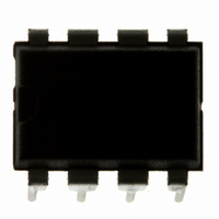
MC9S08QG4MPAE Freescale Semiconductor, MC9S08QG4MPAE Datasheet - Page 145

MC9S08QG4MPAE
Manufacturer Part Number
MC9S08QG4MPAE
Description
IC MCU 4K FLASH 8-PDIP
Manufacturer
Freescale Semiconductor
Series
HCS08r
Datasheet
1.MC9S08QG8CDTER.pdf
(314 pages)
Specifications of MC9S08QG4MPAE
Core Processor
HCS08
Core Size
8-Bit
Speed
20MHz
Connectivity
I²C, SCI, SPI
Peripherals
LVD, POR, PWM, WDT
Number Of I /o
4
Program Memory Size
4KB (4K x 8)
Program Memory Type
FLASH
Ram Size
256 x 8
Voltage - Supply (vcc/vdd)
1.8 V ~ 3.6 V
Data Converters
A/D 4x10b
Oscillator Type
Internal
Operating Temperature
-40°C ~ 125°C
Package / Case
8-DIP (0.300", 7.62mm)
Controller Family/series
HCS08
No. Of I/o's
6
Ram Memory Size
256Byte
Cpu Speed
20MHz
No. Of Timers
2
Embedded Interface Type
I2C, SCI, SPI
Rohs Compliant
Yes
Processor Series
S08QG
Core
HCS08
Data Bus Width
8 bit
Data Ram Size
256 B
Interface Type
I2C, SCI, SPI
Maximum Clock Frequency
20 MHz
Number Of Programmable I/os
12
Number Of Timers
1
Maximum Operating Temperature
+ 125 C
Mounting Style
Through Hole
3rd Party Development Tools
EWS08
Development Tools By Supplier
DEMO9S08QG8E
Minimum Operating Temperature
- 40 C
On-chip Adc
10 bit, 8 Channel
Lead Free Status / RoHS Status
Lead free / RoHS Compliant
Eeprom Size
-
Lead Free Status / Rohs Status
Details
- Current page: 145 of 314
- Download datasheet (6Mb)
Chapter 10
Internal Clock Source (S08ICSV1)
10.1
The internal clock source (ICS) module provides clock source choices for the MCU. The module contains
a frequency-locked loop (FLL) as a clock source that is controllable by either an internal or an external
reference clock. The module can provide this FLL clock or either of the internal or external reference
clocks as a source for the MCU system clock. There are also signals provided to control a low power
oscillator (XOSC) module to allow the use of an external crystal/resonator as the external reference clock.
Whichever clock source is chosen, it is passed through a reduced bus divider (BDIV) which allows a lower
final output clock frequency to be derived.
The bus frequency will be one-half of the ICSOUT frequency.
10.1.1
When the internal reference is enabled in stop mode (IREFSTEN = 1), the voltage regulator must also be
enabled in stop mode by setting the LVDE and LVDSE bits in the SPMSC1 register.
On this MCU, the internal reference is not connected to any module that is operational in stop mode.
Therefore, the IREFSTEN bit in the ICSC1 register should always be cleared.
Figure 10-1
10.1.2
A factory trim value is stored in FLASH during production testing. To be used, this value must be copied
from FLASH memory to the ICSTRM register. A factory value for this FTRIM bit is also stored in FLASH
and must be copied into the FTRIM bit in the ICSSC register. See
the factory ICSTRM and FTRIM values.
Freescale Semiconductor
Introduction
Module Configuration
Factory Trim Value
shows the MC9S08QG8/4 block diagram with the ICS highlighted.
The external reference clock is not available on all packages. See
for external clock availability for each package option.
MC9S08QG8 and MC9S08QG4 Data Sheet, Rev. 5
NOTE
Table 4-4
for the FLASH locations of
Table 1-1
143
Related parts for MC9S08QG4MPAE
Image
Part Number
Description
Manufacturer
Datasheet
Request
R
Part Number:
Description:
Manufacturer:
Freescale Semiconductor, Inc
Datasheet:
Part Number:
Description:
Manufacturer:
Freescale Semiconductor, Inc
Datasheet:
Part Number:
Description:
Manufacturer:
Freescale Semiconductor, Inc
Datasheet:
Part Number:
Description:
Manufacturer:
Freescale Semiconductor, Inc
Datasheet:
Part Number:
Description:
Manufacturer:
Freescale Semiconductor, Inc
Datasheet:
Part Number:
Description:
Manufacturer:
Freescale Semiconductor, Inc
Datasheet:
Part Number:
Description:
Manufacturer:
Freescale Semiconductor, Inc
Datasheet:
Part Number:
Description:
Manufacturer:
Freescale Semiconductor, Inc
Datasheet:
Part Number:
Description:
Manufacturer:
Freescale Semiconductor, Inc
Datasheet:
Part Number:
Description:
Manufacturer:
Freescale Semiconductor, Inc
Datasheet:
Part Number:
Description:
Manufacturer:
Freescale Semiconductor, Inc
Datasheet:
Part Number:
Description:
Manufacturer:
Freescale Semiconductor, Inc
Datasheet:
Part Number:
Description:
Manufacturer:
Freescale Semiconductor, Inc
Datasheet:
Part Number:
Description:
Manufacturer:
Freescale Semiconductor, Inc
Datasheet:
Part Number:
Description:
Manufacturer:
Freescale Semiconductor, Inc
Datasheet:


