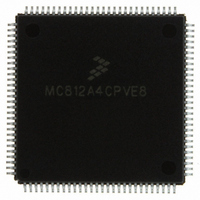
MC812A4CPVE8 Freescale Semiconductor, MC812A4CPVE8 Datasheet - Page 129

MC812A4CPVE8
Manufacturer Part Number
MC812A4CPVE8
Description
IC MCU 16BIT EEPROM 4K 112-LQFP
Manufacturer
Freescale Semiconductor
Series
HC12r
Datasheet
1.MC812A4CPVE8.pdf
(242 pages)
Specifications of MC812A4CPVE8
Core Processor
CPU12
Core Size
16-Bit
Speed
8MHz
Connectivity
SCI, SPI
Peripherals
POR, WDT
Number Of I /o
83
Program Memory Size
4KB (4K x 8)
Program Memory Type
EEPROM
Ram Size
1K x 8
Voltage - Supply (vcc/vdd)
4.5 V ~ 5.5 V
Data Converters
A/D 8x8b
Oscillator Type
Internal
Operating Temperature
-40°C ~ 85°C
Package / Case
112-LQFP
Processor Series
HC812A
Core
HC12
Data Bus Width
16 bit
Data Ram Size
1 KB
Interface Type
SCI, SPI
Maximum Clock Frequency
8 MHz
Number Of Programmable I/os
91
Number Of Timers
8
Maximum Operating Temperature
+ 85 C
Mounting Style
SMD/SMT
Minimum Operating Temperature
- 40 C
On-chip Adc
8 bit, 8 Channel
Controller Family/series
68HC12
No. Of I/o's
91
Eeprom Memory Size
4KB
Ram Memory Size
1KB
Cpu Speed
8MHz
No. Of Timers
1
Rohs Compliant
Yes
Lead Free Status / RoHS Status
Lead free / RoHS Compliant
Eeprom Size
-
Lead Free Status / Rohs Status
Details
Available stocks
Company
Part Number
Manufacturer
Quantity
Price
Company:
Part Number:
MC812A4CPVE8
Manufacturer:
MOTOLOLA
Quantity:
672
Company:
Part Number:
MC812A4CPVE8
Manufacturer:
Freescale Semiconductor
Quantity:
10 000
Part Number:
MC812A4CPVE8
Manufacturer:
NXP/恩智浦
Quantity:
20 000
Company:
Part Number:
MC812A4CPVE80
Manufacturer:
SHARP
Quantity:
5 510
12.5.7 Timer Control Registers 1 and 2
Read: Anytime
Write: Anytime
OMx/OLx — Output Mode/Output Level Bits
Channel 7 shares a pin with the pulse accumulator input pin. To use the PAI input, clear both the OM7
and OL7 bits and clear the OC7M7 bit in the output compare 7 mask register.
Freescale Semiconductor
These bit pairs select the output action to be taken as a result of a successful output compare. When
either OMx or OLx is set and the IOSx bit is set, the pin is an output regardless of the state of the
corresponding DDRT bit.
Address: $0088
Address: $0089
Reset:
Reset:
Read:
Read:
Write:
Write:
OM7
OM3
Bit 7
Bit 7
0
0
OMx:OLx
Table 12-1. Selection of Output Compare Action
Figure 12-12. Timer Control Register 1 (TCTL1)
Figure 12-13. Timer Control Register 2 (TCTL2)
00
01
10
11
OL7
OL3
6
0
6
0
MC68HC812A4 Data Sheet, Rev. 7
Timer disconnected from output pin logic
Toggle OCn output line
Clear OCn output line
Set OCn output line
OM6
OM2
5
0
5
0
Action on Output Compare
OL6
OL2
4
0
4
0
OM5
OM1
3
0
3
0
OL5
OL1
2
0
2
0
Registers and Reset Initialization
OM4
OM0
1
0
1
0
Bit 0
Bit 0
OL4
OL0
0
0
129


