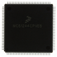
MC812A4CPVE8 Freescale Semiconductor, MC812A4CPVE8 Datasheet - Page 183

MC812A4CPVE8
Manufacturer Part Number
MC812A4CPVE8
Description
IC MCU 16BIT EEPROM 4K 112-LQFP
Manufacturer
Freescale Semiconductor
Series
HC12r
Datasheet
1.MC812A4CPVE8.pdf
(242 pages)
Specifications of MC812A4CPVE8
Core Processor
CPU12
Core Size
16-Bit
Speed
8MHz
Connectivity
SCI, SPI
Peripherals
POR, WDT
Number Of I /o
83
Program Memory Size
4KB (4K x 8)
Program Memory Type
EEPROM
Ram Size
1K x 8
Voltage - Supply (vcc/vdd)
4.5 V ~ 5.5 V
Data Converters
A/D 8x8b
Oscillator Type
Internal
Operating Temperature
-40°C ~ 85°C
Package / Case
112-LQFP
Processor Series
HC812A
Core
HC12
Data Bus Width
16 bit
Data Ram Size
1 KB
Interface Type
SCI, SPI
Maximum Clock Frequency
8 MHz
Number Of Programmable I/os
91
Number Of Timers
8
Maximum Operating Temperature
+ 85 C
Mounting Style
SMD/SMT
Minimum Operating Temperature
- 40 C
On-chip Adc
8 bit, 8 Channel
Controller Family/series
68HC12
No. Of I/o's
91
Eeprom Memory Size
4KB
Ram Memory Size
1KB
Cpu Speed
8MHz
No. Of Timers
1
Rohs Compliant
Yes
Lead Free Status / RoHS Status
Lead free / RoHS Compliant
Eeprom Size
-
Lead Free Status / Rohs Status
Details
Available stocks
Company
Part Number
Manufacturer
Quantity
Price
Company:
Part Number:
MC812A4CPVE8
Manufacturer:
MOTOLOLA
Quantity:
672
Company:
Part Number:
MC812A4CPVE8
Manufacturer:
Freescale Semiconductor
Quantity:
10 000
Part Number:
MC812A4CPVE8
Manufacturer:
NXP/恩智浦
Quantity:
20 000
Company:
Part Number:
MC812A4CPVE80
Manufacturer:
SHARP
Quantity:
5 510
becomes set, the byte from the master transfers to the SPI data register. The byte remains in a read buffer
until replaced by the next byte from the master.
15.5.3 Baud Rate Generation
A clock divider in the SPI produces eight divided P-clock signals. The P-clock divisors are 2, 4, 8, 16, 32,
64, 128, and 256. The SPR[2:1:0] bits select one of the divided P-clock signals to control the rate of the
shift register. Through the SCK pin, the selected clock signal also controls the rate of the shift register of
the slave SPI or other slave peripheral.
The clock divider is active only in master mode and only when a transmission is taking place. Otherwise,
the divider is disabled to save power.
15.5.4 Clock Phase and Polarity
The clock phase and clock polarity bits, CPHA and CPOL, can select any of four combinations of serial
clock phase and polarity. The CPHA bit determines whether a falling SS edge or the first SCK edge begins
the transmission. The CPOL bit determines whether SCK is active-high or active-low.
When CPHA = 0, a falling SS edge signals the slave to begin transmission. The capture strobe for the
first bit occurs on the first serial clock edge. Therefore, the slave must begin driving its data before the
first serial clock edge. After transmission of all eight bits, the slave SS pin must toggle from low to high to
low again to begin another transmission. This format may be preferable in systems having more than one
slave driving the master MISO line.
Freescale Semiconductor
CAPTURE STROBE
MINIMUM t
MSB FIRST (LSBF = 0)
LSB FIRST (LSBF = 1)
FROM MASTER
TRANSFER
FROM SLAVE
SCK CYCLES
L
, t
BEGIN
TO SLAVE
T
CPOL = 0
CPOL = 1
, and t
To transmit between SPI modules, both modules must have identical CPHA
and CPOL values.
MOSI
MISO
SCK
SCK
I
SS
= 1/2 SCK CYCLE
t
L
MSB
LSB
1
Figure 15-4. Transmission Format 0 (CPHA = 0)
BIT 6
BIT 1
2
MC68HC812A4 Data Sheet, Rev. 7
BIT 5
BIT 2
3
NOTE
BIT 4
BIT 3
4
BIT 3
BIT 4
5
BIT 2
BIT 5
6
BIT 1
BIT 6
7
TRANSFER
END
MSB
LSB
8
Functional Description
t
T
t
I
183


