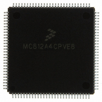
MC812A4CPVE8 Freescale Semiconductor, MC812A4CPVE8 Datasheet - Page 166

MC812A4CPVE8
Manufacturer Part Number
MC812A4CPVE8
Description
IC MCU 16BIT EEPROM 4K 112-LQFP
Manufacturer
Freescale Semiconductor
Series
HC12r
Datasheet
1.MC812A4CPVE8.pdf
(242 pages)
Specifications of MC812A4CPVE8
Core Processor
CPU12
Core Size
16-Bit
Speed
8MHz
Connectivity
SCI, SPI
Peripherals
POR, WDT
Number Of I /o
83
Program Memory Size
4KB (4K x 8)
Program Memory Type
EEPROM
Ram Size
1K x 8
Voltage - Supply (vcc/vdd)
4.5 V ~ 5.5 V
Data Converters
A/D 8x8b
Oscillator Type
Internal
Operating Temperature
-40°C ~ 85°C
Package / Case
112-LQFP
Processor Series
HC812A
Core
HC12
Data Bus Width
16 bit
Data Ram Size
1 KB
Interface Type
SCI, SPI
Maximum Clock Frequency
8 MHz
Number Of Programmable I/os
91
Number Of Timers
8
Maximum Operating Temperature
+ 85 C
Mounting Style
SMD/SMT
Minimum Operating Temperature
- 40 C
On-chip Adc
8 bit, 8 Channel
Controller Family/series
68HC12
No. Of I/o's
91
Eeprom Memory Size
4KB
Ram Memory Size
1KB
Cpu Speed
8MHz
No. Of Timers
1
Rohs Compliant
Yes
Lead Free Status / RoHS Status
Lead free / RoHS Compliant
Eeprom Size
-
Lead Free Status / Rohs Status
Details
Available stocks
Company
Part Number
Manufacturer
Quantity
Price
Company:
Part Number:
MC812A4CPVE8
Manufacturer:
MOTOLOLA
Quantity:
672
Company:
Part Number:
MC812A4CPVE8
Manufacturer:
Freescale Semiconductor
Quantity:
10 000
Part Number:
MC812A4CPVE8
Manufacturer:
NXP/恩智浦
Quantity:
20 000
Company:
Part Number:
MC812A4CPVE80
Manufacturer:
SHARP
Quantity:
5 510
Serial Communications Interface Module (SCI)
14.5.5 Single-Wire Operation
Normally, the SCI uses two pins for transmitting and receiving. In single-wire operation, the RXD pin is
disconnected from the SCI and is available as a general-purpose I/O pin. The SCI uses the TXD pin for
both receiving and transmitting.
Setting the data direction bit for the TXD pin configures TXD as the output for transmitted data. Clearing
the data direction bit configures TXD as the input for received data.
166
•
the message is addressed process the frames that follow. Any receiver for which a message is not
addressed can set its RWU bit and return to the standby state. The RWU bit remains set and the
receiver remains on standby until another idle character appears on the RXD pin.
Idle line wakeup requires that messages be separated by at least one idle character and that no
message contains idle characters.
The idle character that wakes a receiver does not set the receiver idle flag, IDLE, or the receive
data register full flag, RDRF.
The idle line type bit, ILT, determines whether the receiver begins counting logic 1s as idle
character bits after the start bit or after the stop bit. ILT is in SCI control register 1 (SCCR1).
Address mark wakeup (WAKE = 1) — In this wakeup method, a logic 1 in the most significant bit
(MSB) position of a frame clears the RWU bit and wakes up the SCI. The logic 1 in the MSB
position marks a frame as an address frame that contains addressing information. All receivers
evaluate the addressing information, and the receivers for which the message is addressed
process the frames that follow. Any receiver for which a message is not addressed can set its RWU
bit and return to the standby state. The RWU bit remains set and the receiver remains on standby
until another address frame appears on the RXD pin.
The logic 1 MSB of an address frame clears the receiver’s RWU bit before the stop bit is received
and sets the RDRF flag.
Address mark wakeup allows messages to contain idle characters but requires that the MSB be
reserved for use in address frames.
With the WAKE bit clear, setting the RWU bit after the RXD pin has been
idle can cause the receiver to wake up immediately.
Figure 14-15. Single-Wire Operation (LOOPS = 1 and RSRC = 1)
DDRS BIT = 1
DDRS BIT = 0
TRANSMITTER
TRANSMITTER
RECEIVER
RECEIVER
MC68HC812A4 Data Sheet, Rev. 7
NOTE
WOMS
NC
RXD
RXD
TXD
TXD
GENERAL-
PURPOSE I/O
GENERAL-
PURPOSE I/O
Freescale Semiconductor


