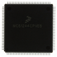
MC812A4CPVE8 Freescale Semiconductor, MC812A4CPVE8 Datasheet - Page 217

MC812A4CPVE8
Manufacturer Part Number
MC812A4CPVE8
Description
IC MCU 16BIT EEPROM 4K 112-LQFP
Manufacturer
Freescale Semiconductor
Series
HC12r
Datasheet
1.MC812A4CPVE8.pdf
(242 pages)
Specifications of MC812A4CPVE8
Core Processor
CPU12
Core Size
16-Bit
Speed
8MHz
Connectivity
SCI, SPI
Peripherals
POR, WDT
Number Of I /o
83
Program Memory Size
4KB (4K x 8)
Program Memory Type
EEPROM
Ram Size
1K x 8
Voltage - Supply (vcc/vdd)
4.5 V ~ 5.5 V
Data Converters
A/D 8x8b
Oscillator Type
Internal
Operating Temperature
-40°C ~ 85°C
Package / Case
112-LQFP
Processor Series
HC812A
Core
HC12
Data Bus Width
16 bit
Data Ram Size
1 KB
Interface Type
SCI, SPI
Maximum Clock Frequency
8 MHz
Number Of Programmable I/os
91
Number Of Timers
8
Maximum Operating Temperature
+ 85 C
Mounting Style
SMD/SMT
Minimum Operating Temperature
- 40 C
On-chip Adc
8 bit, 8 Channel
Controller Family/series
68HC12
No. Of I/o's
91
Eeprom Memory Size
4KB
Ram Memory Size
1KB
Cpu Speed
8MHz
No. Of Timers
1
Rohs Compliant
Yes
Lead Free Status / RoHS Status
Lead free / RoHS Compliant
Eeprom Size
-
Lead Free Status / Rohs Status
Details
Available stocks
Company
Part Number
Manufacturer
Quantity
Price
Company:
Part Number:
MC812A4CPVE8
Manufacturer:
MOTOLOLA
Quantity:
672
Company:
Part Number:
MC812A4CPVE8
Manufacturer:
Freescale Semiconductor
Quantity:
10 000
Part Number:
MC812A4CPVE8
Manufacturer:
NXP/恩智浦
Quantity:
20 000
Company:
Part Number:
MC812A4CPVE80
Manufacturer:
SHARP
Quantity:
5 510
17.4 BDM Registers
Seven BDM registers are mapped into the standard 64-Kbyte address space when BDM is active. The
registers can be accessed with the hardware READ_BD and WRITE_BD commands, but must not be
written during BDM operation. Most users are only interested in the STATUS register at $FF01; other
registers are for use only by BDM firmware and logic.
The instruction register is discussed for two conditions:
17.4.1 BDM Instruction Register
This section describes the BDM instruction register under hardware command and firmware command.
17.4.1.1 Hardware Command
The bits in the BDM instruction register have the following meanings when a hardware command is
executed.
H/F — Hardware/Firmware Flag
DATA — Data Flag
R/W — Read/Write Flag
BKGND — Hardware Request Bit to Enter Active Background Mode
W/B — Word/Byte Transfer Flag
BD/U — BDM Map/User Map Flag
Freescale Semiconductor
•
•
Indicates whether BDM registers and ROM are mapped to addresses $FF00 to $FFFF in the standard
64-Kbyte address space. Used only by hardware read/write commands.
1 = Hardware instruction
0 = Firmware instruction
1 = Data included in command
0 = No data
0 = Write
1 = Read
1 = Hardware background command (INSTRUCTION = $90)
0 = Not a hardware background command
1 = Word transfer
0 = Byte transfer
1 = BDM resources in map
0 = BDM resources not in map
When a hardware command is executed
When a firmware command is executed
Address: $FF00
Reset:
Read:
Write:
Bit 7
Figure 17-4. BDM Instruction Register (INSTRUCTION)
H/F
0
DATA
6
0
MC68HC812A4 Data Sheet, Rev. 7
R/W
5
0
BKGND
4
0
W/B
3
0
BD/U
2
0
1
0
0
Bit 0
0
0
BDM Registers
217


