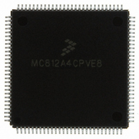
MC812A4CPVE8 Freescale Semiconductor, MC812A4CPVE8 Datasheet - Page 86

MC812A4CPVE8
Manufacturer Part Number
MC812A4CPVE8
Description
IC MCU 16BIT EEPROM 4K 112-LQFP
Manufacturer
Freescale Semiconductor
Series
HC12r
Datasheet
1.MC812A4CPVE8.pdf
(242 pages)
Specifications of MC812A4CPVE8
Core Processor
CPU12
Core Size
16-Bit
Speed
8MHz
Connectivity
SCI, SPI
Peripherals
POR, WDT
Number Of I /o
83
Program Memory Size
4KB (4K x 8)
Program Memory Type
EEPROM
Ram Size
1K x 8
Voltage - Supply (vcc/vdd)
4.5 V ~ 5.5 V
Data Converters
A/D 8x8b
Oscillator Type
Internal
Operating Temperature
-40°C ~ 85°C
Package / Case
112-LQFP
Processor Series
HC812A
Core
HC12
Data Bus Width
16 bit
Data Ram Size
1 KB
Interface Type
SCI, SPI
Maximum Clock Frequency
8 MHz
Number Of Programmable I/os
91
Number Of Timers
8
Maximum Operating Temperature
+ 85 C
Mounting Style
SMD/SMT
Minimum Operating Temperature
- 40 C
On-chip Adc
8 bit, 8 Channel
Controller Family/series
68HC12
No. Of I/o's
91
Eeprom Memory Size
4KB
Ram Memory Size
1KB
Cpu Speed
8MHz
No. Of Timers
1
Rohs Compliant
Yes
Lead Free Status / RoHS Status
Lead free / RoHS Compliant
Eeprom Size
-
Lead Free Status / Rohs Status
Details
Available stocks
Company
Part Number
Manufacturer
Quantity
Price
Company:
Part Number:
MC812A4CPVE8
Manufacturer:
MOTOLOLA
Quantity:
672
Company:
Part Number:
MC812A4CPVE8
Manufacturer:
Freescale Semiconductor
Quantity:
10 000
Part Number:
MC812A4CPVE8
Manufacturer:
NXP/恩智浦
Quantity:
20 000
Company:
Part Number:
MC812A4CPVE80
Manufacturer:
SHARP
Quantity:
5 510
Memory Expansion and Chip-Select
8.4.3 Port F Data Direction Register
Read: Anytime
Write: Anytime
When port F is active, DDRF determines pin direction.
8.4.4 Port G Data Direction Register
Read: Anytime
Write: Anytime
When port G is active, DDRG determines pin direction.
8.4.5 Data Page Register
Read: Anytime
Write: Anytime
When enabled (DWEN = 1), the value in this register determines which of the 256 4-Kbyte pages is active
in the data window. An access to the data page memory area ($7000 to $7FFF) forces the contents of
DPAGE to address pins ADDR15–ADDR12 and expansion address pins ADDR19–ADDR16. Bits
ADDR20 and ADDR21 are forced to 1 if enabled by MXAR. Data chip-select (CSD) must be used in
conjunction with this memory expansion window.
86
1 = Associated bit is an output.
0 = Associated bit is an input.
1 = Associated bit is an output.
0 = Associated bit is an input.
Address: $0032
Address: $0033
Address: $0034
Reset:
Reset:
Reset:
Read:
Read:
Read:
Write:
Write:
Write:
PD19
Bit 7
Bit 7
Bit 7
0
0
0
0
0
Figure 8-10. Port G Data Direction Register (DDRG)
Figure 8-9. Port F Data Direction Register (DDRF)
= Unimplemented
= Unimplemented
Figure 8-11. Data Page Register (DPAGE)
DDRF6
PD18
6
0
6
0
0
6
0
MC68HC812A4 Data Sheet, Rev. 7
DDRG5
DDRF5
PD17
5
0
5
0
5
0
DDRG4
DDRF4
PD16
4
0
4
0
4
0
DDRG3
DDRF3
PD15
3
0
3
0
3
0
DDRG2
DDRF2
PD14
2
0
2
0
2
0
DDRG1
DDRF1
PD13
1
0
1
0
1
0
Freescale Semiconductor
DDRF0
DDRG0
PD12
Bit 0
Bit 0
Bit 0
0
0
0


