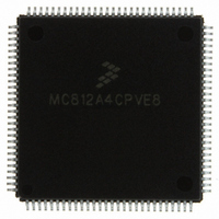
MC812A4CPVE8 Freescale Semiconductor, MC812A4CPVE8 Datasheet - Page 215

MC812A4CPVE8
Manufacturer Part Number
MC812A4CPVE8
Description
IC MCU 16BIT EEPROM 4K 112-LQFP
Manufacturer
Freescale Semiconductor
Series
HC12r
Datasheet
1.MC812A4CPVE8.pdf
(242 pages)
Specifications of MC812A4CPVE8
Core Processor
CPU12
Core Size
16-Bit
Speed
8MHz
Connectivity
SCI, SPI
Peripherals
POR, WDT
Number Of I /o
83
Program Memory Size
4KB (4K x 8)
Program Memory Type
EEPROM
Ram Size
1K x 8
Voltage - Supply (vcc/vdd)
4.5 V ~ 5.5 V
Data Converters
A/D 8x8b
Oscillator Type
Internal
Operating Temperature
-40°C ~ 85°C
Package / Case
112-LQFP
Processor Series
HC812A
Core
HC12
Data Bus Width
16 bit
Data Ram Size
1 KB
Interface Type
SCI, SPI
Maximum Clock Frequency
8 MHz
Number Of Programmable I/os
91
Number Of Timers
8
Maximum Operating Temperature
+ 85 C
Mounting Style
SMD/SMT
Minimum Operating Temperature
- 40 C
On-chip Adc
8 bit, 8 Channel
Controller Family/series
68HC12
No. Of I/o's
91
Eeprom Memory Size
4KB
Ram Memory Size
1KB
Cpu Speed
8MHz
No. Of Timers
1
Rohs Compliant
Yes
Lead Free Status / RoHS Status
Lead free / RoHS Compliant
Eeprom Size
-
Lead Free Status / Rohs Status
Details
Available stocks
Company
Part Number
Manufacturer
Quantity
Price
Company:
Part Number:
MC812A4CPVE8
Manufacturer:
MOTOLOLA
Quantity:
672
Company:
Part Number:
MC812A4CPVE8
Manufacturer:
Freescale Semiconductor
Quantity:
10 000
Part Number:
MC812A4CPVE8
Manufacturer:
NXP/恩智浦
Quantity:
20 000
Company:
Part Number:
MC812A4CPVE80
Manufacturer:
SHARP
Quantity:
5 510
BDM becomes active at the next instruction boundary following execution of the BDM BACKGROUND
command, but tags activate BDM before a tagged instruction is executed.
In special single-chip mode, background operation is enabled and active immediately out of reset. This
active case replaces the M68HC11 boot function and allows programming a system with blank memory.
While BDM is active, a set of BDM control registers are mapped to addresses $FF00 to $FF06. The BDM
control logic uses these registers which can be read anytime by BDM logic, not user programs. Refer to
17.4 BDM Registers
Some on-chip peripherals have a BDM control bit which allows suspending the peripheral function during
BDM. For example, if the timer control is enabled, the timer counter is stopped while in BDM. Once normal
program flow is continued, the timer counter is re-enabled to simulate real-time operations.
17.3.3 BDM Commands
All BDM command opcodes are eight bits long and can be followed by an address and/or data, as
indicated by the instruction. These commands do not require the CPU to be in active BDM mode for
execution.
The host controller must wait 150 cycles for a non-intrusive BDM command to execute before another
command can be sent. This delay includes 128 cycles for the maximum delay for a dead cycle. For data
read commands, the host must insert this delay between sending the address and attempting to read the
data.
BDM logic retains control of the internal buses until a read or write is completed. If an operation can be
completed in a single cycle, it does not intrude on normal CPU operation. However, if an operation
requires multiple cycles, CPU clocks are frozen until the operation is complete.
The CPU must be in background mode to execute commands that are implemented in the BDM ROM.
The BDM ROM is located at $FF20 to $FFFF while BDM is active. There are also seven bytes of BDM
registers which are located at $FF00 to $FF06 while BDM is active. The CPU executes code from this
ROM to perform the requested operation. These commands are shown in
Freescale Semiconductor
READ_BD_WORD
READ_BD_BYTE
BACKGROUND
READ_BYTE
Command
STATUS
(1)
for detailed descriptions.
Table 17-2. BDM Commands Implemented in Hardware
Opcode (Hex)
EC
E4
E4
E0
90
MC68HC812A4 Data Sheet, Rev. 7
1000 0000 (out)
0000 0000 (out)
1100 0000 (out)
16-bit data out
16-bit data out
16-bit address
16-bit address
16-bit address
16-bit data out
FF01,
FF01,
FF01,
None
Data
Enter background mode, if firmware is enabled.
Read from memory with BDM in map (may steal cycles if
external access); data for odd address on low byte, data for
even address on high byte
READ_BD_BYTE $FF01. Running user code; BGND
instruction is not allowed
READ_BD_BYTE $FF01. BGND instruction is allowed.
READ_BD_BYTE $FF01. Background mode active,
waiting for single wire serial command
Read from memory with BDM in map (may steal cycles if
external access); must be aligned access
Read from memory with BDM out of map (may steal cycles
if external access); data for odd address on low byte, data
for even address on high byte
Table 17-2
Description
Background Debug Mode (BDM)
and
Table
17-3.
215


