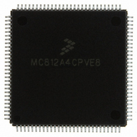
MC812A4CPVE8 Freescale Semiconductor, MC812A4CPVE8 Datasheet - Page 148

MC812A4CPVE8
Manufacturer Part Number
MC812A4CPVE8
Description
IC MCU 16BIT EEPROM 4K 112-LQFP
Manufacturer
Freescale Semiconductor
Series
HC12r
Datasheet
1.MC812A4CPVE8.pdf
(242 pages)
Specifications of MC812A4CPVE8
Core Processor
CPU12
Core Size
16-Bit
Speed
8MHz
Connectivity
SCI, SPI
Peripherals
POR, WDT
Number Of I /o
83
Program Memory Size
4KB (4K x 8)
Program Memory Type
EEPROM
Ram Size
1K x 8
Voltage - Supply (vcc/vdd)
4.5 V ~ 5.5 V
Data Converters
A/D 8x8b
Oscillator Type
Internal
Operating Temperature
-40°C ~ 85°C
Package / Case
112-LQFP
Processor Series
HC812A
Core
HC12
Data Bus Width
16 bit
Data Ram Size
1 KB
Interface Type
SCI, SPI
Maximum Clock Frequency
8 MHz
Number Of Programmable I/os
91
Number Of Timers
8
Maximum Operating Temperature
+ 85 C
Mounting Style
SMD/SMT
Minimum Operating Temperature
- 40 C
On-chip Adc
8 bit, 8 Channel
Controller Family/series
68HC12
No. Of I/o's
91
Eeprom Memory Size
4KB
Ram Memory Size
1KB
Cpu Speed
8MHz
No. Of Timers
1
Rohs Compliant
Yes
Lead Free Status / RoHS Status
Lead free / RoHS Compliant
Eeprom Size
-
Lead Free Status / Rohs Status
Details
Available stocks
Company
Part Number
Manufacturer
Quantity
Price
Company:
Part Number:
MC812A4CPVE8
Manufacturer:
MOTOLOLA
Quantity:
672
Company:
Part Number:
MC812A4CPVE8
Manufacturer:
Freescale Semiconductor
Quantity:
10 000
Part Number:
MC812A4CPVE8
Manufacturer:
NXP/恩智浦
Quantity:
20 000
Company:
Part Number:
MC812A4CPVE80
Manufacturer:
SHARP
Quantity:
5 510
Multiple Serial Interface (MSI)
13.6.2 Port S Data Direction Register
Read: Anytime
Write: Anytime
DDRS7–DDRS0 — Port S Data Direction Bits
13.6.3 Port S Pullup and Reduced Drive Control
Read: Anytime
Write: Anytime
PUPS — Pullup Port S Enable Bit
148
These bits control the data direction of each port S pin. Setting a DDRS bit makes the pin an output;
clearing a DDRS bit makes the pin an input. Reset clears the port S data direction register, configuring
all port S pins as inputs.
Setting PUPS enables internal pullup devices on all port S input pins. If a pin is programmed as output,
the pullup device becomes inactive.
1 = Corresponding port S pin configured as output
0 = Corresponding port S pin configured as input
1 = Pullups enabled
0 = Pullups disabled
Address: $00D1
Address: $00D7
When the LOOPS bit is clear, the RX pins of SCI0 and SCI1 are inputs and
the TX pins are outputs regardless of their DDRS bits.
When the SPI is enabled, an SPI input pin is an input regardless of its
DDRS bit.
When the SPI is enabled, an SPI output is an output only if its DDRS bit is
set. When the DDRS bit of an SPI output is clear, the pin is available for
general-purpose I/O.
Reset:
Read:
Write:
Reset:
Read:
Write:
DDRS7
Bit 7
Bit 7
0
0
0
Figure 13-4. Port S Data Direction Register (DDRS)
Figure 13-5. SPI Control Register 2 (SP0CR2)
= Unimplemented
DDRS6
6
0
6
0
0
MC68HC812A4 Data Sheet, Rev. 7
DDRS5
5
0
5
0
0
DDRS4
NOTE
4
0
4
0
0
DDRS3
PUPS
3
0
3
1
DDRS2
RDS
2
0
2
0
DDRS1
1
0
1
0
0
Freescale Semiconductor
DDRS0
Bit 0
SPC0
Bit 0
0
0


