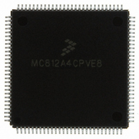
MC812A4CPVE8 Freescale Semiconductor, MC812A4CPVE8 Datasheet - Page 76

MC812A4CPVE8
Manufacturer Part Number
MC812A4CPVE8
Description
IC MCU 16BIT EEPROM 4K 112-LQFP
Manufacturer
Freescale Semiconductor
Series
HC12r
Datasheet
1.MC812A4CPVE8.pdf
(242 pages)
Specifications of MC812A4CPVE8
Core Processor
CPU12
Core Size
16-Bit
Speed
8MHz
Connectivity
SCI, SPI
Peripherals
POR, WDT
Number Of I /o
83
Program Memory Size
4KB (4K x 8)
Program Memory Type
EEPROM
Ram Size
1K x 8
Voltage - Supply (vcc/vdd)
4.5 V ~ 5.5 V
Data Converters
A/D 8x8b
Oscillator Type
Internal
Operating Temperature
-40°C ~ 85°C
Package / Case
112-LQFP
Processor Series
HC812A
Core
HC12
Data Bus Width
16 bit
Data Ram Size
1 KB
Interface Type
SCI, SPI
Maximum Clock Frequency
8 MHz
Number Of Programmable I/os
91
Number Of Timers
8
Maximum Operating Temperature
+ 85 C
Mounting Style
SMD/SMT
Minimum Operating Temperature
- 40 C
On-chip Adc
8 bit, 8 Channel
Controller Family/series
68HC12
No. Of I/o's
91
Eeprom Memory Size
4KB
Ram Memory Size
1KB
Cpu Speed
8MHz
No. Of Timers
1
Rohs Compliant
Yes
Lead Free Status / RoHS Status
Lead free / RoHS Compliant
Eeprom Size
-
Lead Free Status / Rohs Status
Details
Available stocks
Company
Part Number
Manufacturer
Quantity
Price
Company:
Part Number:
MC812A4CPVE8
Manufacturer:
MOTOLOLA
Quantity:
672
Company:
Part Number:
MC812A4CPVE8
Manufacturer:
Freescale Semiconductor
Quantity:
10 000
Part Number:
MC812A4CPVE8
Manufacturer:
NXP/恩智浦
Quantity:
20 000
Company:
Part Number:
MC812A4CPVE80
Manufacturer:
SHARP
Quantity:
5 510
EEPROM
EEVEN — Even Row Programming Bit
MARG — Program and Erase Voltage Margin Test Enable Bit
EECPD — Charge Pump Disable Bit
EECPRD — Charge Pump Ramp Disable Bit
ECPM — Charge Pump Monitor Enable Bit
7.3.4 EEPROM Programming Register
Read: Anytime
Write: Varies from bit to bit
BULKP — Bulk Erase Protection Bit
BYTE — Byte and Aligned Word Erase Bit
ROW — Row or Bulk Erase Bit (when BYTE = 0)
BYTE and ROW have no effect when ERASE = 0.
If BYTE = 1 and test mode is not enabled, only the location specified by the address written to the
programming latches is erased. The operation is a byte or an aligned word erase depending on the size
of written data.
76
This bit is used to evaluate the program/erase voltage margin.
This bit is known to enhance write/erase endurance of EEPROM cells.
Write anytime, if EEPGM = 0 and PROTLCK = 0
Write anytime, if EEPGM = 0
Write anytime, if EEPGM = 0
1 = Bulk program/erase all even rows
0 = Even row bulk programming/erasing disabled
1 = Program and erase margin test
0 = Normal operation
1 = Disable charge pump
0 = Charge pump is turned on during program/erase
1 = Disable charge pump controlled ramp up
0 = Charge pump is turned on progressively during program/erase
1 = Output the charge pump voltage on the IRQ/V
0 = Normal operation
1 = EEPROM protected from bulk or row erase
0 = EEPROM can be bulk erased.
1 = One byte or one aligned word erase only
0 = Bulk or row erase enabled
1 = Erase only one 32-byte row
0 = Erase entire EEPROM array
Address: $00F3
Reset:
Read:
Write:
BULKP
Figure 7-5. EEPROM Programming Register (EEPROG)
Bit 7
1
6
0
0
MC68HC812A4 Data Sheet, Rev. 7
5
0
0
BYTE
4
0
PP
ROW
pin
3
0
ERASE
2
0
EELAT
1
0
Freescale Semiconductor
EEPGM
Bit 0
0


