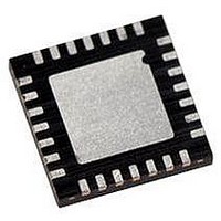
PIC18LF27J53-I/ML Microchip Technology, PIC18LF27J53-I/ML Datasheet - Page 104

PIC18LF27J53-I/ML
Manufacturer Part Number
PIC18LF27J53-I/ML
Description
IC PIC MCU 128KB FLASH 28QFN
Manufacturer
Microchip Technology
Series
PIC® XLP™ 18Fr
Datasheets
1.PIC18LF24J10-ISS.pdf
(32 pages)
2.PIC18F26J13-ISS.pdf
(496 pages)
3.PIC18F26J53-ISS.pdf
(586 pages)
4.PIC18F26J53-ISS.pdf
(12 pages)
Specifications of PIC18LF27J53-I/ML
Core Size
8-Bit
Program Memory Size
128KB (64K x 16)
Core Processor
PIC
Speed
48MHz
Connectivity
I²C, LIN, SPI, UART/USART, USB
Peripherals
Brown-out Detect/Reset, POR, PWM, WDT
Number Of I /o
22
Program Memory Type
FLASH
Ram Size
3.8K x 8
Voltage - Supply (vcc/vdd)
2 V ~ 2.75 V
Data Converters
A/D 10x10b/12b
Oscillator Type
Internal
Operating Temperature
-40°C ~ 85°C
Package / Case
*
Controller Family/series
PIC18
Cpu Speed
48MHz
Digital Ic Case Style
QFN
Supply Voltage Range
1.8V To 3.6V
Embedded Interface Type
I2C, SPI, USART
Rohs Compliant
Yes
Lead Free Status / RoHS Status
Lead free / RoHS Compliant
Eeprom Size
-
Lead Free Status / RoHS Status
Lead free / RoHS Compliant, Lead free / RoHS Compliant
Available stocks
Company
Part Number
Manufacturer
Quantity
Price
Company:
Part Number:
PIC18LF27J53-I/ML
Manufacturer:
ATMEL
Quantity:
101
- PIC18LF24J10-ISS PDF datasheet
- PIC18F26J13-ISS PDF datasheet #2
- PIC18F26J53-ISS PDF datasheet #3
- PIC18F26J53-ISS PDF datasheet #4
- Current page: 104 of 586
- Download datasheet (6Mb)
PIC18F47J53 FAMILY
6.4.3.1
At the core of Indirect Addressing are three sets of
registers: FSR0, FSR1 and FSR2. Each represents a
pair of 8-bit registers, FSRnH and FSRnL. The four
upper bits of the FSRnH register are not used, so each
FSR pair holds a 12-bit value. This represents a value
that can address the entire range of the data memory
in a linear fashion. The FSR register pairs, then, serve
as pointers to data memory locations.
Indirect Addressing is accomplished with a set of INDF
operands, INDF0 through INDF2. These can be pre-
sumed as “virtual” registers; they are mapped in the
FIGURE 6-8:
DS39964B-page 104
Using an instruction with one of the
Indirect Addressing registers as the
operand....
...uses the 12-bit address stored in
the FSR pair associated with that
register....
...to determine the data memory
location to be used in that operation.
In this case, the FSR1 pair contains
FCCh. This means the contents of
location, FCCh, will be added to that
of the W register and stored back in
FCCh.
FSR Registers and the INDF
Operand (INDF)
INDIRECT ADDRESSING
x x x x 1 1 1 1
7
ADDWF
Preliminary
FSR1H:FSR1L
,
INDF1
0
7
1 1 0 0 1 1 0 0
,
SFR space but are not physically implemented. Read-
ing or writing to a particular INDF register actually
accesses its corresponding FSR register pair. A read
from INDF1, for example, reads the data at the address
indicated by FSR1H:FSR1L. Instructions that use the
INDF registers as operands actually use the contents
of their corresponding FSR as a pointer to the instruc-
tion’s target. The INDF operand is just a convenient
way of using the pointer.
Because Indirect Addressing uses a full 12-bit address,
data RAM banking is not necessary. Thus, the current
contents of the BSR and the Access RAM bit have no
effect on determining the target address.
1
0
2010 Microchip Technology Inc.
FFFh
E00h
F00h
000h
100h
200h
300h
Data Memory
Bank 13
Bank 14
Bank 15
through
Bank 0
Bank 1
Bank 2
Bank 3
Related parts for PIC18LF27J53-I/ML
Image
Part Number
Description
Manufacturer
Datasheet
Request
R

Part Number:
Description:
Manufacturer:
Microchip Technology Inc.
Datasheet:

Part Number:
Description:
Manufacturer:
Microchip Technology Inc.
Datasheet:

Part Number:
Description:
Manufacturer:
Microchip Technology Inc.
Datasheet:

Part Number:
Description:
Manufacturer:
Microchip Technology Inc.
Datasheet:

Part Number:
Description:
Manufacturer:
Microchip Technology Inc.
Datasheet:

Part Number:
Description:
Manufacturer:
Microchip Technology Inc.
Datasheet:

Part Number:
Description:
Manufacturer:
Microchip Technology Inc.
Datasheet:

Part Number:
Description:
Manufacturer:
Microchip Technology Inc.
Datasheet:


