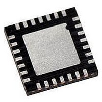
PIC18LF27J53-I/ML Microchip Technology, PIC18LF27J53-I/ML Datasheet - Page 119

PIC18LF27J53-I/ML
Manufacturer Part Number
PIC18LF27J53-I/ML
Description
IC PIC MCU 128KB FLASH 28QFN
Manufacturer
Microchip Technology
Series
PIC® XLP™ 18Fr
Datasheets
1.PIC18LF24J10-ISS.pdf
(32 pages)
2.PIC18F26J13-ISS.pdf
(496 pages)
3.PIC18F26J53-ISS.pdf
(586 pages)
4.PIC18F26J53-ISS.pdf
(12 pages)
Specifications of PIC18LF27J53-I/ML
Core Size
8-Bit
Program Memory Size
128KB (64K x 16)
Core Processor
PIC
Speed
48MHz
Connectivity
I²C, LIN, SPI, UART/USART, USB
Peripherals
Brown-out Detect/Reset, POR, PWM, WDT
Number Of I /o
22
Program Memory Type
FLASH
Ram Size
3.8K x 8
Voltage - Supply (vcc/vdd)
2 V ~ 2.75 V
Data Converters
A/D 10x10b/12b
Oscillator Type
Internal
Operating Temperature
-40°C ~ 85°C
Package / Case
*
Controller Family/series
PIC18
Cpu Speed
48MHz
Digital Ic Case Style
QFN
Supply Voltage Range
1.8V To 3.6V
Embedded Interface Type
I2C, SPI, USART
Rohs Compliant
Yes
Lead Free Status / RoHS Status
Lead free / RoHS Compliant
Eeprom Size
-
Lead Free Status / RoHS Status
Lead free / RoHS Compliant, Lead free / RoHS Compliant
Available stocks
Company
Part Number
Manufacturer
Quantity
Price
Company:
Part Number:
PIC18LF27J53-I/ML
Manufacturer:
ATMEL
Quantity:
101
- PIC18LF24J10-ISS PDF datasheet
- PIC18F26J13-ISS PDF datasheet #2
- PIC18F26J53-ISS PDF datasheet #3
- PIC18F26J53-ISS PDF datasheet #4
- Current page: 119 of 586
- Download datasheet (6Mb)
8.0
8.1
All PIC18 devices include an 8 x 8 hardware multiplier
as part of the ALU. The multiplier performs an unsigned
operation and yields a 16-bit result that is stored in the
product register pair, PRODH:PRODL. The multiplier’s
operation does not affect any flags in the STATUS
register.
Making multiplication a hardware operation allows it to
be completed in a single instruction cycle. This has the
advantages of higher computational throughput and
reduced code size for multiplication algorithms and
allows the PIC18 devices to be used in many applica-
tions previously reserved for digital signal processors.
Table 8-1 provides a comparison of various hardware
and software multiply operations, along with the
savings in memory and execution time.
8.2
Example 8-1 provides the instruction sequence for an
8 x 8 unsigned multiplication. Only one instruction is
required when one of the arguments is already loaded
in the WREG register.
Example 8-2 provides the instruction sequence for an
8 x 8 signed multiplication. To account for the sign bits
of the arguments, each argument’s Most Significant bit
(MSb) is tested and the appropriate subtractions are
done.
TABLE 8-1:
2010 Microchip Technology Inc.
16 x 16 unsigned
8 x 8 unsigned
16 x 16 signed
8 x 8 signed
Routine
8 x 8 HARDWARE MULTIPLIER
Introduction
Operation
PERFORMANCE COMPARISON FOR VARIOUS MULTIPLY OPERATIONS
Without hardware multiply
Without hardware multiply
Without hardware multiply
Without hardware multiply
Hardware multiply
Hardware multiply
Hardware multiply
Hardware multiply
Multiply Method
Preliminary
Program
Memory
(Words)
13
33
21
28
52
35
1
6
PIC18F47J53 FAMILY
EXAMPLE 8-1:
EXAMPLE 8-2:
MOVF
MULWF
MOVF
MULWF
BTFSC
SUBWF
MOVF
BTFSC
SUBWF
Cycles
(Max)
242
254
69
91
28
40
1
6
ARG1, W
ARG2
ARG1, W
ARG2
ARG2, SB
PRODH, F
ARG2, W
ARG1, SB
PRODH, F
@ 48 MHz
20.1 s
21.6 s
83.3 ns
500 ns
5.7 s
7.5 s
2.3 s
3.3 s
8 x 8 UNSIGNED MULTIPLY
ROUTINE
8 x 8 SIGNED MULTIPLY
ROUTINE
;
; ARG1 * ARG2 ->
; PRODH:PRODL
; ARG1 * ARG2 ->
; PRODH:PRODL
; Test Sign Bit
; PRODH = PRODH
;
; Test Sign Bit
; PRODH = PRODH
;
@ 10 MHz
102.6 s
27.6 s
36.4 s
96.8 s
16.0 s
11.2 s
Time
400 ns
2.4 s
DS39964B-page 119
- ARG1
- ARG2
@ 4 MHz
242 s
254 s
69 s
91 s
28 s
40 s
1 s
6 s
Related parts for PIC18LF27J53-I/ML
Image
Part Number
Description
Manufacturer
Datasheet
Request
R

Part Number:
Description:
Manufacturer:
Microchip Technology Inc.
Datasheet:

Part Number:
Description:
Manufacturer:
Microchip Technology Inc.
Datasheet:

Part Number:
Description:
Manufacturer:
Microchip Technology Inc.
Datasheet:

Part Number:
Description:
Manufacturer:
Microchip Technology Inc.
Datasheet:

Part Number:
Description:
Manufacturer:
Microchip Technology Inc.
Datasheet:

Part Number:
Description:
Manufacturer:
Microchip Technology Inc.
Datasheet:

Part Number:
Description:
Manufacturer:
Microchip Technology Inc.
Datasheet:

Part Number:
Description:
Manufacturer:
Microchip Technology Inc.
Datasheet:


