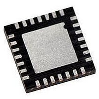
PIC18LF27J53-I/ML Microchip Technology, PIC18LF27J53-I/ML Datasheet - Page 275

PIC18LF27J53-I/ML
Manufacturer Part Number
PIC18LF27J53-I/ML
Description
IC PIC MCU 128KB FLASH 28QFN
Manufacturer
Microchip Technology
Series
PIC® XLP™ 18Fr
Datasheets
1.PIC18LF24J10-ISS.pdf
(32 pages)
2.PIC18F26J13-ISS.pdf
(496 pages)
3.PIC18F26J53-ISS.pdf
(586 pages)
4.PIC18F26J53-ISS.pdf
(12 pages)
Specifications of PIC18LF27J53-I/ML
Core Size
8-Bit
Program Memory Size
128KB (64K x 16)
Core Processor
PIC
Speed
48MHz
Connectivity
I²C, LIN, SPI, UART/USART, USB
Peripherals
Brown-out Detect/Reset, POR, PWM, WDT
Number Of I /o
22
Program Memory Type
FLASH
Ram Size
3.8K x 8
Voltage - Supply (vcc/vdd)
2 V ~ 2.75 V
Data Converters
A/D 10x10b/12b
Oscillator Type
Internal
Operating Temperature
-40°C ~ 85°C
Package / Case
*
Controller Family/series
PIC18
Cpu Speed
48MHz
Digital Ic Case Style
QFN
Supply Voltage Range
1.8V To 3.6V
Embedded Interface Type
I2C, SPI, USART
Rohs Compliant
Yes
Lead Free Status / RoHS Status
Lead free / RoHS Compliant
Eeprom Size
-
Lead Free Status / RoHS Status
Lead free / RoHS Compliant, Lead free / RoHS Compliant
Available stocks
Company
Part Number
Manufacturer
Quantity
Price
Company:
Part Number:
PIC18LF27J53-I/ML
Manufacturer:
ATMEL
Quantity:
101
- PIC18LF24J10-ISS PDF datasheet
- PIC18F26J13-ISS PDF datasheet #2
- PIC18F26J53-ISS PDF datasheet #3
- PIC18F26J53-ISS PDF datasheet #4
- Current page: 275 of 586
- Download datasheet (6Mb)
19.4
The Enhanced PWM mode can generate a PWM signal
on up to four different output pins with up to 10 bits of
resolution. It can do this through four different PWM
Output modes:
• Single PWM mode
• Half-Bridge PWM mode
• Full-Bridge PWM, Forward mode
• Full-Bridge PWM, Reverse mode
To select an Enhanced PWM mode, the PxM bits of the
CCPxCON register must be set appropriately.
FIGURE 19-3:
2010 Microchip Technology Inc.
Note 1: The TRIS register value for each PWM output must be configured appropriately.
Note 1: The 8-bit timer TMR2 register is concatenated with the 2-bit internal Q clock, or 2 bits of the prescaler, to
2: Any pin not used by an Enhanced PWM mode is available for alternate pin functions.
PWM (Enhanced Mode)
CCPR1H (Slave)
Duty Cycle Registers
Comparator
CCPR1L
PR2
TMR2
Comparator
create the 10-bit time base.
SIMPLIFIED BLOCK DIAGRAM OF THE ENHANCED PWM MODE EXAMPLE
(1)
Clear Timer2,
toggle PWM pin and
latch duty cycle
DC1B<1:0>
R
S
PxM<1:0>
Q
Preliminary
ECCP1DEL
Controller
ECCPx/PxA
Output
PIC18F47J53 FAMILY
2
The PWM outputs are multiplexed with I/O pins and are
designated: PxA, PxB, PxC and PxD. The polarity of the
PWM pins is configurable and is selected by setting the
CCPxM bits in the CCPxCON register appropriately.
Table 19-1 provides the pin assignments for each
Enhanced PWM mode.
Figure 19-3 provides an example of a simplified block
diagram of the Enhanced PWM module.
Note:
PxC
PxD
PxB
4
CCPxM<3:0>
To
incomplete waveform when the PWM is
first enabled, the ECCP module waits until
the start of a new PWM period before
generating a PWM signal.
TRIS
TRIS
TRIS
TRIS
prevent
the
generation
ECCPx/Output Pi
Output Pi
Output Pi
Output Pi
DS39964B-page 275
n
n
n
of
n
an
Related parts for PIC18LF27J53-I/ML
Image
Part Number
Description
Manufacturer
Datasheet
Request
R

Part Number:
Description:
Manufacturer:
Microchip Technology Inc.
Datasheet:

Part Number:
Description:
Manufacturer:
Microchip Technology Inc.
Datasheet:

Part Number:
Description:
Manufacturer:
Microchip Technology Inc.
Datasheet:

Part Number:
Description:
Manufacturer:
Microchip Technology Inc.
Datasheet:

Part Number:
Description:
Manufacturer:
Microchip Technology Inc.
Datasheet:

Part Number:
Description:
Manufacturer:
Microchip Technology Inc.
Datasheet:

Part Number:
Description:
Manufacturer:
Microchip Technology Inc.
Datasheet:

Part Number:
Description:
Manufacturer:
Microchip Technology Inc.
Datasheet:


