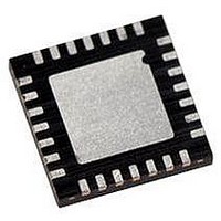
PIC18LF27J53-I/ML Microchip Technology, PIC18LF27J53-I/ML Datasheet - Page 552

PIC18LF27J53-I/ML
Manufacturer Part Number
PIC18LF27J53-I/ML
Description
IC PIC MCU 128KB FLASH 28QFN
Manufacturer
Microchip Technology
Series
PIC® XLP™ 18Fr
Datasheets
1.PIC18LF24J10-ISS.pdf
(32 pages)
2.PIC18F26J13-ISS.pdf
(496 pages)
3.PIC18F26J53-ISS.pdf
(586 pages)
4.PIC18F26J53-ISS.pdf
(12 pages)
Specifications of PIC18LF27J53-I/ML
Core Size
8-Bit
Program Memory Size
128KB (64K x 16)
Core Processor
PIC
Speed
48MHz
Connectivity
I²C, LIN, SPI, UART/USART, USB
Peripherals
Brown-out Detect/Reset, POR, PWM, WDT
Number Of I /o
22
Program Memory Type
FLASH
Ram Size
3.8K x 8
Voltage - Supply (vcc/vdd)
2 V ~ 2.75 V
Data Converters
A/D 10x10b/12b
Oscillator Type
Internal
Operating Temperature
-40°C ~ 85°C
Package / Case
*
Controller Family/series
PIC18
Cpu Speed
48MHz
Digital Ic Case Style
QFN
Supply Voltage Range
1.8V To 3.6V
Embedded Interface Type
I2C, SPI, USART
Rohs Compliant
Yes
Lead Free Status / RoHS Status
Lead free / RoHS Compliant
Eeprom Size
-
Lead Free Status / RoHS Status
Lead free / RoHS Compliant, Lead free / RoHS Compliant
Available stocks
Company
Part Number
Manufacturer
Quantity
Price
Company:
Part Number:
PIC18LF27J53-I/ML
Manufacturer:
ATMEL
Quantity:
101
- PIC18LF24J10-ISS PDF datasheet
- PIC18F26J13-ISS PDF datasheet #2
- PIC18F26J53-ISS PDF datasheet #3
- PIC18F26J53-ISS PDF datasheet #4
- Current page: 552 of 586
- Download datasheet (6Mb)
PIC18F47J53 FAMILY
TABLE 31-31: 10-BIT A/D CONVERSION REQUIREMENTS
TABLE 31-32: 12-BIT A/D CONVERSION REQUIREMENTS
DS39964B-page 552
130
131
132
135
137
Note 1:
130
131
132
135
137
Note 1:
Param
Param
No.
No.
2:
3:
4:
2:
3:
4:
T
T
T
T
T
T
T
T
T
T
Symbol
Symbol
AD
CNV
ACQ
SWC
AD
CNV
ACQ
SWC
DIS
DIS
The time of the A/D clock period is dependent on the device frequency and the T
ADRES registers may be read on the following T
The time for the holding capacitor to acquire the “New” input voltage when the voltage changes full scale after the con-
version (V
On the following cycle of the device clock.
The time of the A/D clock period is dependent on the device frequency and the T
ADRES registers may be read on the following T
The time for the holding capacitor to acquire the “New” input voltage when the voltage changes full scale
after the conversion (V
On the following cycle of the device clock.
A/D Clock Period
Conversion Time
(not including acquisition time)
Acquisition Time
Switching Time from Convert Sample
Discharge Time
A/D Clock Period
Conversion Time
(not including acquisition time)
Acquisition Time
Switching Time from Convert Sample
Discharge Time
DD
to V
SS
or V
Characteristic
Characteristic
SS
DD
(3)
(3)
to V
to V
DD
SS
). The source impedance (R
or V
SS
(2)
(2)
Preliminary
to V
CY
DD
cycle.
). The source impedance (R
CY
cycle.
Min
Min
0.7
1.4
0.2
0.8
1.4
0.2
13
11
—
—
S
) on the input channels is 50W.
(Note 4)
(Note 4)
25.0
12.5
Max
Max
12
14
—
—
—
—
(1)
(1)
Units
Units
AD
T
T
s
s
s
s
s
s
AD
AD
clock divider.
S
2010 Microchip Technology Inc.
) on the input channels is 50.
T
-40C to +85C
T
OSC
OSC
AD
based, V
based, V
clock divider.
Conditions
Conditions
REF
REF
3.0V
3.0V
Related parts for PIC18LF27J53-I/ML
Image
Part Number
Description
Manufacturer
Datasheet
Request
R

Part Number:
Description:
Manufacturer:
Microchip Technology Inc.
Datasheet:

Part Number:
Description:
Manufacturer:
Microchip Technology Inc.
Datasheet:

Part Number:
Description:
Manufacturer:
Microchip Technology Inc.
Datasheet:

Part Number:
Description:
Manufacturer:
Microchip Technology Inc.
Datasheet:

Part Number:
Description:
Manufacturer:
Microchip Technology Inc.
Datasheet:

Part Number:
Description:
Manufacturer:
Microchip Technology Inc.
Datasheet:

Part Number:
Description:
Manufacturer:
Microchip Technology Inc.
Datasheet:

Part Number:
Description:
Manufacturer:
Microchip Technology Inc.
Datasheet:


