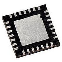
PIC18LF27J53-I/ML Microchip Technology, PIC18LF27J53-I/ML Datasheet - Page 58

PIC18LF27J53-I/ML
Manufacturer Part Number
PIC18LF27J53-I/ML
Description
IC PIC MCU 128KB FLASH 28QFN
Manufacturer
Microchip Technology
Series
PIC® XLP™ 18Fr
Datasheets
1.PIC18LF24J10-ISS.pdf
(32 pages)
2.PIC18F26J13-ISS.pdf
(496 pages)
3.PIC18F26J53-ISS.pdf
(586 pages)
4.PIC18F26J53-ISS.pdf
(12 pages)
Specifications of PIC18LF27J53-I/ML
Core Size
8-Bit
Program Memory Size
128KB (64K x 16)
Core Processor
PIC
Speed
48MHz
Connectivity
I²C, LIN, SPI, UART/USART, USB
Peripherals
Brown-out Detect/Reset, POR, PWM, WDT
Number Of I /o
22
Program Memory Type
FLASH
Ram Size
3.8K x 8
Voltage - Supply (vcc/vdd)
2 V ~ 2.75 V
Data Converters
A/D 10x10b/12b
Oscillator Type
Internal
Operating Temperature
-40°C ~ 85°C
Package / Case
*
Controller Family/series
PIC18
Cpu Speed
48MHz
Digital Ic Case Style
QFN
Supply Voltage Range
1.8V To 3.6V
Embedded Interface Type
I2C, SPI, USART
Rohs Compliant
Yes
Lead Free Status / RoHS Status
Lead free / RoHS Compliant
Eeprom Size
-
Lead Free Status / RoHS Status
Lead free / RoHS Compliant, Lead free / RoHS Compliant
Available stocks
Company
Part Number
Manufacturer
Quantity
Price
Company:
Part Number:
PIC18LF27J53-I/ML
Manufacturer:
ATMEL
Quantity:
101
- PIC18LF24J10-ISS PDF datasheet
- PIC18F26J13-ISS PDF datasheet #2
- PIC18F26J53-ISS PDF datasheet #3
- PIC18F26J53-ISS PDF datasheet #4
- Current page: 58 of 586
- Download datasheet (6Mb)
PIC18F47J53 FAMILY
4.6.9
Deep
Register 4-1 through Register 4-6.
REGISTER 4-1:
REGISTER 4-2:
DS39964B-page 58
bit 7
Legend:
R = Readable bit
-n = Value at POR
bit 7
bit 6-3
bit 2
bit 1
bit 0
Note 1:
bit 7
Legend:
R = Readable bit
-n = Value at POR
bit 7-3
bit 2
bit 1
bit 0
Note 1:
DSEN
R/W-0
U-0
—
Sleep
(1)
In order to enter Deep Sleep, Sleep must be executed immediately after setting DSEN.
This is the value when V
DEEP SLEEP MODE REGISTERS
mode
DSEN: Deep Sleep Enable bit
1 = Deep Sleep mode is entered on a SLEEP command
0 = Sleep mode is entered on a SLEEP command
Unimplemented: Read as ‘0’
(Reserved): Always write ‘0’ to this bit
DSULPEN: Ultra Low-Power Wake-up Module Enable bit
1 = ULPWU module is enabled in Deep Sleep
0 = ULPWU module is disabled in Deep Sleep
RTCWDIS: RTCC Wake-up Disable bit
1 = Wake-up from RTCC is disabled
0 = Wake-up from RTCC is enabled
Unimplemented: Read as ‘0’
ULPWDIS: Ultra Low-Power Wake-up Disable bit
1 = ULPWU wake-up source is disabled
0 = ULPWU wake-up source is enabled (must also set DSULPEN = 1)
DSBOR: Deep Sleep BOR Event Status bit
1 = DSBOREN was enabled and V
0 = DSBOREN was disabled or V
RELEASE: I/O Pin State Release bit
Upon waking from Deep Sleep, the I/O pins maintain their previous states. Clearing this bit will
release the I/O pins and allow their respective TRIS and LAT bits to control their states.
but did not fall below V
Sleep
U-0
U-0
—
—
DSCONH: DEEP SLEEP CONTROL HIGH BYTE REGISTER (BANKED F4Dh)
DSCONL: DEEP SLEEP LOW BYTE CONTROL REGISTER (BANKED F4Ch)
registers
r = Reserved bit
W = Writable bit
W = Writable bit
‘1’ = Bit is set
‘1’ = Bit is set
are
U-0
U-0
DD
—
—
is initially applied.
provided
DSBOR
(1)
U-0
U-0
Preliminary
—
—
DD
DD
in
dropped below the DSBOR arming voltage during Deep Sleep,
did not drop below the DSBOR arming voltage during Deep
U = Unimplemented bit, read as ‘0’
‘0’ = Bit is cleared
U = Unimplemented bit, read as ‘0’
‘0’ = Bit is cleared
U-0
U-0
—
—
ULPWDIS
R/W-0
r-0
r
2010 Microchip Technology Inc.
x = Bit is unknown
x = Bit is unknown
DSULPEN
R/W-0
DSBOR
R/W-0
(1)
RTCWDIS
RELEASE
R/W-0
R/W-0
(1)
bit 0
bit 0
Related parts for PIC18LF27J53-I/ML
Image
Part Number
Description
Manufacturer
Datasheet
Request
R

Part Number:
Description:
Manufacturer:
Microchip Technology Inc.
Datasheet:

Part Number:
Description:
Manufacturer:
Microchip Technology Inc.
Datasheet:

Part Number:
Description:
Manufacturer:
Microchip Technology Inc.
Datasheet:

Part Number:
Description:
Manufacturer:
Microchip Technology Inc.
Datasheet:

Part Number:
Description:
Manufacturer:
Microchip Technology Inc.
Datasheet:

Part Number:
Description:
Manufacturer:
Microchip Technology Inc.
Datasheet:

Part Number:
Description:
Manufacturer:
Microchip Technology Inc.
Datasheet:

Part Number:
Description:
Manufacturer:
Microchip Technology Inc.
Datasheet:


