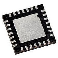
PIC18LF27J53-I/ML Microchip Technology, PIC18LF27J53-I/ML Datasheet - Page 373

PIC18LF27J53-I/ML
Manufacturer Part Number
PIC18LF27J53-I/ML
Description
IC PIC MCU 128KB FLASH 28QFN
Manufacturer
Microchip Technology
Series
PIC® XLP™ 18Fr
Datasheets
1.PIC18LF24J10-ISS.pdf
(32 pages)
2.PIC18F26J13-ISS.pdf
(496 pages)
3.PIC18F26J53-ISS.pdf
(586 pages)
4.PIC18F26J53-ISS.pdf
(12 pages)
Specifications of PIC18LF27J53-I/ML
Core Size
8-Bit
Program Memory Size
128KB (64K x 16)
Core Processor
PIC
Speed
48MHz
Connectivity
I²C, LIN, SPI, UART/USART, USB
Peripherals
Brown-out Detect/Reset, POR, PWM, WDT
Number Of I /o
22
Program Memory Type
FLASH
Ram Size
3.8K x 8
Voltage - Supply (vcc/vdd)
2 V ~ 2.75 V
Data Converters
A/D 10x10b/12b
Oscillator Type
Internal
Operating Temperature
-40°C ~ 85°C
Package / Case
*
Controller Family/series
PIC18
Cpu Speed
48MHz
Digital Ic Case Style
QFN
Supply Voltage Range
1.8V To 3.6V
Embedded Interface Type
I2C, SPI, USART
Rohs Compliant
Yes
Lead Free Status / RoHS Status
Lead free / RoHS Compliant
Eeprom Size
-
Lead Free Status / RoHS Status
Lead free / RoHS Compliant, Lead free / RoHS Compliant
Available stocks
Company
Part Number
Manufacturer
Quantity
Price
Company:
Part Number:
PIC18LF27J53-I/ML
Manufacturer:
ATMEL
Quantity:
101
- PIC18LF24J10-ISS PDF datasheet
- PIC18F26J13-ISS PDF datasheet #2
- PIC18F26J53-ISS PDF datasheet #3
- PIC18F26J53-ISS PDF datasheet #4
- Current page: 373 of 586
- Download datasheet (6Mb)
After the A/D module has been configured as desired,
the selected channel must be acquired before the
conversion is started. The analog input channels must
have their corresponding TRIS bits selected as inputs.
To determine acquisition time, see Section 22.1 “A/D
Acquisition Requirements”. After this acquisition
time has elapsed, the A/D conversion can be started.
An acquisition time can be programmed to occur
between setting the GO/DONE bit and the actual start
of the conversion.
The following steps should be followed to do an A/D
conversion:
1.
FIGURE 22-2:
2010 Microchip Technology Inc.
Configure the A/D module:
• Configure the required ADC pins as analog
• Set voltage reference using ADCON0
• Select A/D input channel (ADCON0)
• Select A/D acquisition time (ADCON1)
• Select A/D conversion clock (ADCON1)
• Turn on A/D module (ADCON0)
pins using ANCON0, ANCON1
Legend: C
V
AIN
R
S
V
I
R
SS
C
R
LEAKAGE
T
PIN
IC
HOLD
SS
ANALOG INPUT MODEL
ANx
C
5 pF
PIN
= Input Capacitance
= Threshold Voltage
= Leakage Current at the pin due to
= Interconnect Resistance
= Sampling Switch
= Sample/Hold Capacitance (from DAC)
= Sampling Switch Resistance
various junctions
V
DD
V
V
T
T
= 0.6V
= 0.6V
Preliminary
PIC18F47J53 FAMILY
I
±100 nA
LEAKAGE
2.
3.
4.
5.
6.
7.
R
IC
Configure A/D interrupt (if desired):
• Clear ADIF bit
• Set ADIE bit
• Set GIE bit
Wait the required acquisition time (if required).
Start conversion:
• Set GO/DONE bit (ADCON0<1>)
Wait for A/D conversion to complete, by either:
• Polling for the GO/DONE bit to be cleared
OR
• Waiting for the A/D interrupt
Read A/D Result registers (ADRESH:ADRESL);
clear bit, ADIF, if required.
For the next conversion, go to step 1 or step 2,
as required. The A/D conversion time per bit is
defined as T
required before the next acquisition starts.
1k
SS
Sampling
Switch
V
DD
AD
R
SS
. A minimum Wait of 2 T
Sampling Switch
1
V
SS
C
2
HOLD
3
DS39964B-page 373
= 25 pF
(k)
4
AD
is
Related parts for PIC18LF27J53-I/ML
Image
Part Number
Description
Manufacturer
Datasheet
Request
R

Part Number:
Description:
Manufacturer:
Microchip Technology Inc.
Datasheet:

Part Number:
Description:
Manufacturer:
Microchip Technology Inc.
Datasheet:

Part Number:
Description:
Manufacturer:
Microchip Technology Inc.
Datasheet:

Part Number:
Description:
Manufacturer:
Microchip Technology Inc.
Datasheet:

Part Number:
Description:
Manufacturer:
Microchip Technology Inc.
Datasheet:

Part Number:
Description:
Manufacturer:
Microchip Technology Inc.
Datasheet:

Part Number:
Description:
Manufacturer:
Microchip Technology Inc.
Datasheet:

Part Number:
Description:
Manufacturer:
Microchip Technology Inc.
Datasheet:


