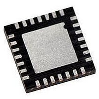
PIC18LF27J53-I/ML Microchip Technology, PIC18LF27J53-I/ML Datasheet - Page 454

PIC18LF27J53-I/ML
Manufacturer Part Number
PIC18LF27J53-I/ML
Description
IC PIC MCU 128KB FLASH 28QFN
Manufacturer
Microchip Technology
Series
PIC® XLP™ 18Fr
Datasheets
1.PIC18LF24J10-ISS.pdf
(32 pages)
2.PIC18F26J13-ISS.pdf
(496 pages)
3.PIC18F26J53-ISS.pdf
(586 pages)
4.PIC18F26J53-ISS.pdf
(12 pages)
Specifications of PIC18LF27J53-I/ML
Core Size
8-Bit
Program Memory Size
128KB (64K x 16)
Core Processor
PIC
Speed
48MHz
Connectivity
I²C, LIN, SPI, UART/USART, USB
Peripherals
Brown-out Detect/Reset, POR, PWM, WDT
Number Of I /o
22
Program Memory Type
FLASH
Ram Size
3.8K x 8
Voltage - Supply (vcc/vdd)
2 V ~ 2.75 V
Data Converters
A/D 10x10b/12b
Oscillator Type
Internal
Operating Temperature
-40°C ~ 85°C
Package / Case
*
Controller Family/series
PIC18
Cpu Speed
48MHz
Digital Ic Case Style
QFN
Supply Voltage Range
1.8V To 3.6V
Embedded Interface Type
I2C, SPI, USART
Rohs Compliant
Yes
Lead Free Status / RoHS Status
Lead free / RoHS Compliant
Eeprom Size
-
Lead Free Status / RoHS Status
Lead free / RoHS Compliant, Lead free / RoHS Compliant
Available stocks
Company
Part Number
Manufacturer
Quantity
Price
Company:
Part Number:
PIC18LF27J53-I/ML
Manufacturer:
ATMEL
Quantity:
101
- PIC18LF24J10-ISS PDF datasheet
- PIC18F26J13-ISS PDF datasheet #2
- PIC18F26J53-ISS PDF datasheet #3
- PIC18F26J53-ISS PDF datasheet #4
- Current page: 454 of 586
- Download datasheet (6Mb)
PIC18F47J53 FAMILY
FIGURE 28-2:
DS39964B-page 454
OR
PIC18LFXXJ53 Devices (Regulator Disabled):
PIC18FXXJ53 Devices (Regulator Enabled):
2.5V
C
F
3.3V
2.5V
3.3V
CONNECTIONS FOR THE
ON-CHIP REGULATOR
V
V
V
V
V
V
V
V
V
DD
DDCORE
SS
DD
DDCORE
SS
DD
DDCORE
SS
PIC18LFXXJ53
PIC18LFXXJ53
PIC18FXXJ53
/V
/V
/V
CAP
CAP
CAP
Preliminary
28.3.2
When the on-chip regulator is enabled, PIC18F47J53
family devices also have a simple brown-out capability.
If the voltage supplied to the regulator is inadequate to
maintain a minimum output level, the regulator Reset
circuitry will generate a Brown-out Reset (BOR). This
event is captured by the BOR flag bit (RCON<0>).
The operation of the BOR is described in more detail in
Section 5.4
Section 5.4.1 “Detecting BOR”. The brown-out voltage
levels are specific in Section 31.1 “DC Characteristics:
Supply Voltage PIC18F47J53 Family (Industrial)”.
28.3.3
The on-chip regulator is designed to meet the power-up
requirements for the device. If the application does not
use the regulator, then strict power-up conditions must
be adhered to. While powering up, V
exceed V
28.3.4
When enabled, the on-chip regulator always consumes
a small incremental amount of current over I
includes when the device is in Sleep mode, even
though the core digital logic does not require much
power. To provide additional savings in applications
where power resources are critical, the regulator can
be configured to automatically enter a lower quiescent
draw Standby mode whenever the device goes into
Sleep mode. This feature is controlled by the REGSLP
bit (WDTCON<7>, Register 28-11). If this bit is set
upon entry into Sleep mode, the regulator will transition
into a lower power state. In this state, the regulator still
provides a regulated output voltage necessary to
maintain SRAM state information, but consumes less
quiescent current.
Substantial Sleep mode power savings can be
obtained by setting the REGSLP bit, but device
wake-up time will increase in order to insure the
regulator has enough time to stabilize.
DD
ON-CHIP REGULATOR AND BOR
POWER-UP REQUIREMENTS
OPERATION IN SLEEP MODE
by 0.3 volts.
“Brown-out
2010 Microchip Technology Inc.
Reset
DDCORE
(BOR)”
should not
DD
. This
and
Related parts for PIC18LF27J53-I/ML
Image
Part Number
Description
Manufacturer
Datasheet
Request
R

Part Number:
Description:
Manufacturer:
Microchip Technology Inc.
Datasheet:

Part Number:
Description:
Manufacturer:
Microchip Technology Inc.
Datasheet:

Part Number:
Description:
Manufacturer:
Microchip Technology Inc.
Datasheet:

Part Number:
Description:
Manufacturer:
Microchip Technology Inc.
Datasheet:

Part Number:
Description:
Manufacturer:
Microchip Technology Inc.
Datasheet:

Part Number:
Description:
Manufacturer:
Microchip Technology Inc.
Datasheet:

Part Number:
Description:
Manufacturer:
Microchip Technology Inc.
Datasheet:

Part Number:
Description:
Manufacturer:
Microchip Technology Inc.
Datasheet:


