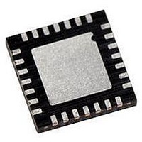
PIC18LF27J53-I/ML Microchip Technology, PIC18LF27J53-I/ML Datasheet - Page 547

PIC18LF27J53-I/ML
Manufacturer Part Number
PIC18LF27J53-I/ML
Description
IC PIC MCU 128KB FLASH 28QFN
Manufacturer
Microchip Technology
Series
PIC® XLP™ 18Fr
Datasheets
1.PIC18LF24J10-ISS.pdf
(32 pages)
2.PIC18F26J13-ISS.pdf
(496 pages)
3.PIC18F26J53-ISS.pdf
(586 pages)
4.PIC18F26J53-ISS.pdf
(12 pages)
Specifications of PIC18LF27J53-I/ML
Core Size
8-Bit
Program Memory Size
128KB (64K x 16)
Core Processor
PIC
Speed
48MHz
Connectivity
I²C, LIN, SPI, UART/USART, USB
Peripherals
Brown-out Detect/Reset, POR, PWM, WDT
Number Of I /o
22
Program Memory Type
FLASH
Ram Size
3.8K x 8
Voltage - Supply (vcc/vdd)
2 V ~ 2.75 V
Data Converters
A/D 10x10b/12b
Oscillator Type
Internal
Operating Temperature
-40°C ~ 85°C
Package / Case
*
Controller Family/series
PIC18
Cpu Speed
48MHz
Digital Ic Case Style
QFN
Supply Voltage Range
1.8V To 3.6V
Embedded Interface Type
I2C, SPI, USART
Rohs Compliant
Yes
Lead Free Status / RoHS Status
Lead free / RoHS Compliant
Eeprom Size
-
Lead Free Status / RoHS Status
Lead free / RoHS Compliant, Lead free / RoHS Compliant
Available stocks
Company
Part Number
Manufacturer
Quantity
Price
Company:
Part Number:
PIC18LF27J53-I/ML
Manufacturer:
ATMEL
Quantity:
101
- PIC18LF24J10-ISS PDF datasheet
- PIC18F26J13-ISS PDF datasheet #2
- PIC18F26J53-ISS PDF datasheet #3
- PIC18F26J53-ISS PDF datasheet #4
- Current page: 547 of 586
- Download datasheet (6Mb)
TABLE 31-25: I
2010 Microchip Technology Inc.
100
101
102
103
90
91
106
107
92
109
110
D102
Note 1:
Param.
No.
2:
T
T
T
T
T
T
T
T
T
T
T
C
Symbol
SU
SU
SU
AA
HIGH
LOW
R
F
HD
HD
BUF
B
As a transmitter, the device must provide this internal minimum delay time to bridge the undefined region (min. 300 ns)
of the falling edge of SCLx to avoid unintended generation of Start or Stop conditions.
A Fast mode I
must then be met. This will automatically be the case if the device does not stretch the LOW period of the SCLx signal.
If such a device does stretch the LOW period of the SCLx signal, it must output the next data bit to the SDAx line, T
max. + T
released.
:
:
:
:
:
STA
DAT
STO
STA
DAT
2
SU
Clock High Time
Clock Low Time
SDAx and SCLx Rise Time 100 kHz mode
SDAx and SCLx Fall Time 100 kHz mode
Start Condition Setup Time 100 kHz mode
Start Condition Hold Time
Data Input Hold Time
Data Input Setup Time
Stop Condition Setup Time 100 kHz mode
Output Valid from Clock
Bus Free Time
Bus Capacitive Loading
C™ BUS DATA REQUIREMENTS (SLAVE MODE)
:
DAT
2
C™ bus device can be used in a Standard mode I
= 1000 + 250 = 1250 ns (according to the Standard mode I
Characteristic
100 kHz mode
400 kHz mode
MSSP modules
100 kHz mode
400 kHz mode
MSSP modules
400 kHz mode
400 kHz mode
400 kHz mode
100 kHz mode
400 kHz mode
100 kHz mode
400 kHz mode
100 kHz mode
400 kHz mode
400 kHz mode
100 kHz mode
400 kHz mode
100 kHz mode
400 kHz mode
Preliminary
PIC18F47J53 FAMILY
20 + 0.1 C
20 + 0.1 C
1.5 T
1.5 T
Min
250
100
4.0
0.6
4.7
1.3
4.7
0.6
4.0
0.6
4.7
0.6
4.7
1.3
—
—
—
—
—
0
0
CY
CY
2
C bus system, but the requirement, T
B
B
3500
1000
Max
300
300
300
0.9
400
—
—
—
—
—
—
—
—
—
—
—
—
—
—
—
—
—
—
2
C bus specification), before the SCLx line is
Units
pF
s
s
s
s
ns
ns
ns
ns
s
s
s
s
ns
s
ns
ns
s
s
ns
ns
s
s
C
10 to 400 pF
C
10 to 400 pF
Only relevant for Repeated
Start condition
After this period, the first clock
pulse is generated
(Note 2)
(Note 1)
Time the bus must be free
before a new transmission can
start
B
B
is specified to be from
is specified to be from
Conditions
DS39964B-page 547
SU
:
DAT
250 ns,
R
Related parts for PIC18LF27J53-I/ML
Image
Part Number
Description
Manufacturer
Datasheet
Request
R

Part Number:
Description:
Manufacturer:
Microchip Technology Inc.
Datasheet:

Part Number:
Description:
Manufacturer:
Microchip Technology Inc.
Datasheet:

Part Number:
Description:
Manufacturer:
Microchip Technology Inc.
Datasheet:

Part Number:
Description:
Manufacturer:
Microchip Technology Inc.
Datasheet:

Part Number:
Description:
Manufacturer:
Microchip Technology Inc.
Datasheet:

Part Number:
Description:
Manufacturer:
Microchip Technology Inc.
Datasheet:

Part Number:
Description:
Manufacturer:
Microchip Technology Inc.
Datasheet:

Part Number:
Description:
Manufacturer:
Microchip Technology Inc.
Datasheet:


