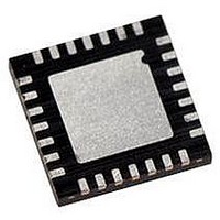
PIC18LF27J53-I/ML Microchip Technology, PIC18LF27J53-I/ML Datasheet - Page 292

PIC18LF27J53-I/ML
Manufacturer Part Number
PIC18LF27J53-I/ML
Description
IC PIC MCU 128KB FLASH 28QFN
Manufacturer
Microchip Technology
Series
PIC® XLP™ 18Fr
Datasheets
1.PIC18LF24J10-ISS.pdf
(32 pages)
2.PIC18F26J13-ISS.pdf
(496 pages)
3.PIC18F26J53-ISS.pdf
(586 pages)
4.PIC18F26J53-ISS.pdf
(12 pages)
Specifications of PIC18LF27J53-I/ML
Core Size
8-Bit
Program Memory Size
128KB (64K x 16)
Core Processor
PIC
Speed
48MHz
Connectivity
I²C, LIN, SPI, UART/USART, USB
Peripherals
Brown-out Detect/Reset, POR, PWM, WDT
Number Of I /o
22
Program Memory Type
FLASH
Ram Size
3.8K x 8
Voltage - Supply (vcc/vdd)
2 V ~ 2.75 V
Data Converters
A/D 10x10b/12b
Oscillator Type
Internal
Operating Temperature
-40°C ~ 85°C
Package / Case
*
Controller Family/series
PIC18
Cpu Speed
48MHz
Digital Ic Case Style
QFN
Supply Voltage Range
1.8V To 3.6V
Embedded Interface Type
I2C, SPI, USART
Rohs Compliant
Yes
Lead Free Status / RoHS Status
Lead free / RoHS Compliant
Eeprom Size
-
Lead Free Status / RoHS Status
Lead free / RoHS Compliant, Lead free / RoHS Compliant
Available stocks
Company
Part Number
Manufacturer
Quantity
Price
Company:
Part Number:
PIC18LF27J53-I/ML
Manufacturer:
ATMEL
Quantity:
101
- PIC18LF24J10-ISS PDF datasheet
- PIC18F26J13-ISS PDF datasheet #2
- PIC18F26J53-ISS PDF datasheet #3
- PIC18F26J53-ISS PDF datasheet #4
- Current page: 292 of 586
- Download datasheet (6Mb)
registers. These include a status register (SSPxSTAT)
PIC18F47J53 FAMILY
20.2
Each MSSP module has three associated control
and two control registers (SSPxCON1 and SSPxCON2).
The use of these registers and their individual Configura-
tion bits differs significantly depending on whether the
MSSP module is operated in SPI or I
Additional details are provided under the individual
sections.
20.3
The SPI mode allows 8 bits of data to be synchronously
transmitted and received simultaneously. All four
modes of SPI are supported.
When MSSP2 is used in SPI mode, it can optionally be
configured to work with the SPI DMA submodule
described in Section 20.4 “SPI DMA Module”.
To accomplish communication, typically three pins are
used:
• Serial Data Out (SDOx) –
• Serial Data In (SDIx) –
• Serial Clock (SCKx) –
Additionally, a fourth pin may be used when in a Slave
mode of operation:
• Slave Select (SSx) – RA5/AN4/C1INC/SS1/
Figure 20-1 depicts the block diagram of the MSSP
module when operating in SPI mode.
DS39964B-page 292
Note:
RC7/CCP10/RX1/DT1/SDO1/RP18 or
SDO2/Remappable
RB5/CCP5/KBI1/SDI1/SDA1/RP8 or
SDI2/Remappable
RB4/CCP4/KBI0/SCK1/SCL1/RP7 or
SCK2/Remappable
HLVDIN/RCV/RP2 or SS2/Remappable
Control Registers
SPI Mode
In devices with more than one MSSP
module, it is very important to pay close
attention to the SSPxCON register names.
SSP1CON1 and
different operational aspects of the same
module,
SSP2CON1 control the same features for
two different modules.
while
SSP1CON2 control
SSP1CON1
2
C mode.
and
Preliminary
FIGURE 20-1:
Note:
SCKx
SDOx
SDIx
SSx
Only port I/O names are used in this diagram for
the sake of brevity. Refer to the text for a full list of
multiplexed functions.
Read
SSx Control
Select
SMP:CKE
Edge
bit 0
Select
Edge
MSSPx BLOCK DIAGRAM
(SPI MODE)
Enable
2010 Microchip Technology Inc.
SSPxBUF reg
TRIS bit
Data to TXx/RXx in SSPxSR
SSPxSR reg
2
Clock Select
SSPM<3:0>
4
2
(
Prescaler
4, 8, 16, 64
TMR2 Output
Write
Clock
Shift
Data Bus
Internal
2
T
OSC
)
Related parts for PIC18LF27J53-I/ML
Image
Part Number
Description
Manufacturer
Datasheet
Request
R

Part Number:
Description:
Manufacturer:
Microchip Technology Inc.
Datasheet:

Part Number:
Description:
Manufacturer:
Microchip Technology Inc.
Datasheet:

Part Number:
Description:
Manufacturer:
Microchip Technology Inc.
Datasheet:

Part Number:
Description:
Manufacturer:
Microchip Technology Inc.
Datasheet:

Part Number:
Description:
Manufacturer:
Microchip Technology Inc.
Datasheet:

Part Number:
Description:
Manufacturer:
Microchip Technology Inc.
Datasheet:

Part Number:
Description:
Manufacturer:
Microchip Technology Inc.
Datasheet:

Part Number:
Description:
Manufacturer:
Microchip Technology Inc.
Datasheet:


