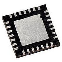
PIC18LF27J53-I/ML Microchip Technology, PIC18LF27J53-I/ML Datasheet - Page 65

PIC18LF27J53-I/ML
Manufacturer Part Number
PIC18LF27J53-I/ML
Description
IC PIC MCU 128KB FLASH 28QFN
Manufacturer
Microchip Technology
Series
PIC® XLP™ 18Fr
Datasheets
1.PIC18LF24J10-ISS.pdf
(32 pages)
2.PIC18F26J13-ISS.pdf
(496 pages)
3.PIC18F26J53-ISS.pdf
(586 pages)
4.PIC18F26J53-ISS.pdf
(12 pages)
Specifications of PIC18LF27J53-I/ML
Core Size
8-Bit
Program Memory Size
128KB (64K x 16)
Core Processor
PIC
Speed
48MHz
Connectivity
I²C, LIN, SPI, UART/USART, USB
Peripherals
Brown-out Detect/Reset, POR, PWM, WDT
Number Of I /o
22
Program Memory Type
FLASH
Ram Size
3.8K x 8
Voltage - Supply (vcc/vdd)
2 V ~ 2.75 V
Data Converters
A/D 10x10b/12b
Oscillator Type
Internal
Operating Temperature
-40°C ~ 85°C
Package / Case
*
Controller Family/series
PIC18
Cpu Speed
48MHz
Digital Ic Case Style
QFN
Supply Voltage Range
1.8V To 3.6V
Embedded Interface Type
I2C, SPI, USART
Rohs Compliant
Yes
Lead Free Status / RoHS Status
Lead free / RoHS Compliant
Eeprom Size
-
Lead Free Status / RoHS Status
Lead free / RoHS Compliant, Lead free / RoHS Compliant
Available stocks
Company
Part Number
Manufacturer
Quantity
Price
Company:
Part Number:
PIC18LF27J53-I/ML
Manufacturer:
ATMEL
Quantity:
101
- PIC18LF24J10-ISS PDF datasheet
- PIC18F26J13-ISS PDF datasheet #2
- PIC18F26J53-ISS PDF datasheet #3
- PIC18F26J53-ISS PDF datasheet #4
- Current page: 65 of 586
- Download datasheet (6Mb)
5.0
The PIC18F47J53 family of devices differentiates
among various kinds of Reset:
a)
b)
c)
d)
e)
f)
g)
h)
i)
j)
This section discusses Resets generated by MCLR,
POR and BOR, and covers the operation of the various
start-up timers.
FIGURE 5-1:
2010 Microchip Technology Inc.
V
Power-on Reset (POR)
MCLR Reset during normal operation
MCLR Reset during power-managed modes
Watchdog
execution)
Configuration Mismatch (CM)
Brown-out Reset (BOR)
RESET Instruction
Stack Full Reset
Stack Underflow Reset
Deep Sleep Reset
Note 1: The V
MCLR
DDCORE
V
DD
RESET
2: The V
Deep Sleep Reset
Pointer
Configuration bit. On “F” devices, the V
CONFIG3L<DSBOREN>.
Sleep mode. The V
Stack
Configuration Word Mismatch
PWRT
Timer
Brown-out
INTRC
( )_IDLE
V
Time-out
32 ms
Reset
DD
Detect
DD
DDCORE
WDT
Sleep
Rise
monitoring BOR circuit can be enabled or disabled on “LF” devices based on the CONFIG3L<DSBOREN>
External Reset
SIMPLIFIED BLOCK DIAGRAM OF ON-CHIP RESET CIRCUIT
Stack Full/Underflow Reset
(1)
RESET Instruction
(WDT)
monitoring BOR circuit is only implemented on “F” devices. It is always used, except while in Deep
POR Pulse
PWRT
DDCORE
Brown-out
11-Bit Ripple Counter
Reset
Reset
(2)
monitoring BOR circuit has a trip point threshold of V
66 ms
(during
DD
Preliminary
monitoring BOR circuit is only enabled during Deep Sleep mode by
PIC18F47J53 FAMILY
For information on WDT Resets, see Section 28.2
“Watchdog Timer (WDT)”. For Stack Reset events,
see Section 6.1.4.4 “Stack Full and Underflow
Resets” and for Deep Sleep mode, see Section 4.6
“Deep Sleep Mode”.
Figure 5-1 provides a simplified block diagram of the
on-chip Reset circuit.
5.1
Device Reset events are tracked through the RCON
register (Register 5-1). The lower five bits of the register
indicate that a specific Reset event has occurred. In
most cases, these bits can only be set by the event and
must be cleared by the application after the event. The
state of these flag bits, taken together, can be read to
indicate the type of Reset that just occurred. This is
described in more detail in Section 5.7 “Reset State of
Registers”.
The RCON register also has a control bit for setting
interrupt priority (IPEN). Interrupt priority is discussed
in Section 9.0 “Interrupts”.
RCON Register
BOR
(parameter D005).
S
R
Q
DS39964B-page 65
Chip_Reset
Related parts for PIC18LF27J53-I/ML
Image
Part Number
Description
Manufacturer
Datasheet
Request
R

Part Number:
Description:
Manufacturer:
Microchip Technology Inc.
Datasheet:

Part Number:
Description:
Manufacturer:
Microchip Technology Inc.
Datasheet:

Part Number:
Description:
Manufacturer:
Microchip Technology Inc.
Datasheet:

Part Number:
Description:
Manufacturer:
Microchip Technology Inc.
Datasheet:

Part Number:
Description:
Manufacturer:
Microchip Technology Inc.
Datasheet:

Part Number:
Description:
Manufacturer:
Microchip Technology Inc.
Datasheet:

Part Number:
Description:
Manufacturer:
Microchip Technology Inc.
Datasheet:

Part Number:
Description:
Manufacturer:
Microchip Technology Inc.
Datasheet:


