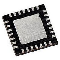
PIC18LF27J53-I/ML Microchip Technology, PIC18LF27J53-I/ML Datasheet - Page 123

PIC18LF27J53-I/ML
Manufacturer Part Number
PIC18LF27J53-I/ML
Description
IC PIC MCU 128KB FLASH 28QFN
Manufacturer
Microchip Technology
Series
PIC® XLP™ 18Fr
Datasheets
1.PIC18LF24J10-ISS.pdf
(32 pages)
2.PIC18F26J13-ISS.pdf
(496 pages)
3.PIC18F26J53-ISS.pdf
(586 pages)
4.PIC18F26J53-ISS.pdf
(12 pages)
Specifications of PIC18LF27J53-I/ML
Core Size
8-Bit
Program Memory Size
128KB (64K x 16)
Core Processor
PIC
Speed
48MHz
Connectivity
I²C, LIN, SPI, UART/USART, USB
Peripherals
Brown-out Detect/Reset, POR, PWM, WDT
Number Of I /o
22
Program Memory Type
FLASH
Ram Size
3.8K x 8
Voltage - Supply (vcc/vdd)
2 V ~ 2.75 V
Data Converters
A/D 10x10b/12b
Oscillator Type
Internal
Operating Temperature
-40°C ~ 85°C
Package / Case
*
Controller Family/series
PIC18
Cpu Speed
48MHz
Digital Ic Case Style
QFN
Supply Voltage Range
1.8V To 3.6V
Embedded Interface Type
I2C, SPI, USART
Rohs Compliant
Yes
Lead Free Status / RoHS Status
Lead free / RoHS Compliant
Eeprom Size
-
Lead Free Status / RoHS Status
Lead free / RoHS Compliant, Lead free / RoHS Compliant
Available stocks
Company
Part Number
Manufacturer
Quantity
Price
Company:
Part Number:
PIC18LF27J53-I/ML
Manufacturer:
ATMEL
Quantity:
101
- PIC18LF24J10-ISS PDF datasheet
- PIC18F26J13-ISS PDF datasheet #2
- PIC18F26J53-ISS PDF datasheet #3
- PIC18F26J53-ISS PDF datasheet #4
- Current page: 123 of 586
- Download datasheet (6Mb)
9.1
The INTCON registers are readable and writable
registers, which contain various enable, priority and
flag bits.
REGISTER 9-1:
2010 Microchip Technology Inc.
bit 7
Legend:
R = Readable bit
-n = Value at POR
bit 7
bit 6
bit 5
bit 4
bit 3
bit 2
bit 1
bit 0
Note 1:
GIE/GIEH
R/W-0
INTCON Registers
A mismatch condition will continue to set this bit. Reading PORTB and waiting 1 T
condition and allow the bit to be cleared.
GIE/GIEH: Global Interrupt Enable bit
When IPEN = 0:
1 = Enables all unmasked interrupts
0 = Disables all interrupts
When IPEN = 1:
1 = Enables all high-priority interrupts
0 = Disables all interrupts
PEIE/GIEL: Peripheral Interrupt Enable bit
When IPEN = 0:
1 = Enables all unmasked peripheral interrupts
0 = Disables all peripheral interrupts
When IPEN = 1:
1 = Enables all low-priority peripheral interrupts
0 = Disables all low-priority peripheral interrupts
TMR0IE: TMR0 Overflow Interrupt Enable bit
1 = Enables the TMR0 overflow interrupt
0 = Disables the TMR0 overflow interrupt
INT0IE: INT0 External Interrupt Enable bit
1 = Enables the INT0 external interrupt
0 = Disables the INT0 external interrupt
RBIE: RB Port Change Interrupt Enable bit
1 = Enables the RB port change interrupt
0 = Disables the RB port change interrupt
TMR0IF: TMR0 Overflow Interrupt Flag bit
1 = The TMR0 register has overflowed (must be cleared in software)
0 = The TMR0 register did not overflow
INT0IF: INT0 External Interrupt Flag bit
1 = The INT0 external interrupt occurred (must be cleared in software)
0 = The INT0 external interrupt did not occur
RBIF: RB Port Change Interrupt Flag bit
1 = At least one of the RB<7:4> pins changed state (must be cleared in software)
0 = None of the RB<7:4> pins have changed state
PEIE/GIEL
R/W-0
INTCON: INTERRUPT CONTROL REGISTER (ACCESS FF2h)
W = Writable bit
‘1’ = Bit is set
TMR0IE
R/W-0
INT0IE
R/W-0
Preliminary
(1)
U = Unimplemented bit, read as ‘0’
‘0’ = Bit is cleared
PIC18F47J53 FAMILY
R/W-0
RBIE
Note:
Interrupt flag bits are set when an interrupt
condition occurs, regardless of the state of
its corresponding enable bit or the global
interrupt enable bit. User software should
ensure the appropriate interrupt flag bits
are clear prior to enabling an interrupt.
This feature allows for software polling.
TMR0IF
R/W-0
x = Bit is unknown
CY
INT0IF
R/W-0
will end the mismatch
DS39964B-page 123
RBIF
R/W-x
(1)
bit 0
Related parts for PIC18LF27J53-I/ML
Image
Part Number
Description
Manufacturer
Datasheet
Request
R

Part Number:
Description:
Manufacturer:
Microchip Technology Inc.
Datasheet:

Part Number:
Description:
Manufacturer:
Microchip Technology Inc.
Datasheet:

Part Number:
Description:
Manufacturer:
Microchip Technology Inc.
Datasheet:

Part Number:
Description:
Manufacturer:
Microchip Technology Inc.
Datasheet:

Part Number:
Description:
Manufacturer:
Microchip Technology Inc.
Datasheet:

Part Number:
Description:
Manufacturer:
Microchip Technology Inc.
Datasheet:

Part Number:
Description:
Manufacturer:
Microchip Technology Inc.
Datasheet:

Part Number:
Description:
Manufacturer:
Microchip Technology Inc.
Datasheet:


