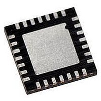
PIC18LF27J53-I/ML Microchip Technology, PIC18LF27J53-I/ML Datasheet - Page 288

PIC18LF27J53-I/ML
Manufacturer Part Number
PIC18LF27J53-I/ML
Description
IC PIC MCU 128KB FLASH 28QFN
Manufacturer
Microchip Technology
Series
PIC® XLP™ 18Fr
Datasheets
1.PIC18LF24J10-ISS.pdf
(32 pages)
2.PIC18F26J13-ISS.pdf
(496 pages)
3.PIC18F26J53-ISS.pdf
(586 pages)
4.PIC18F26J53-ISS.pdf
(12 pages)
Specifications of PIC18LF27J53-I/ML
Core Size
8-Bit
Program Memory Size
128KB (64K x 16)
Core Processor
PIC
Speed
48MHz
Connectivity
I²C, LIN, SPI, UART/USART, USB
Peripherals
Brown-out Detect/Reset, POR, PWM, WDT
Number Of I /o
22
Program Memory Type
FLASH
Ram Size
3.8K x 8
Voltage - Supply (vcc/vdd)
2 V ~ 2.75 V
Data Converters
A/D 10x10b/12b
Oscillator Type
Internal
Operating Temperature
-40°C ~ 85°C
Package / Case
*
Controller Family/series
PIC18
Cpu Speed
48MHz
Digital Ic Case Style
QFN
Supply Voltage Range
1.8V To 3.6V
Embedded Interface Type
I2C, SPI, USART
Rohs Compliant
Yes
Lead Free Status / RoHS Status
Lead free / RoHS Compliant
Eeprom Size
-
Lead Free Status / RoHS Status
Lead free / RoHS Compliant, Lead free / RoHS Compliant
Available stocks
Company
Part Number
Manufacturer
Quantity
Price
Company:
Part Number:
PIC18LF27J53-I/ML
Manufacturer:
ATMEL
Quantity:
101
- PIC18LF24J10-ISS PDF datasheet
- PIC18F26J13-ISS PDF datasheet #2
- PIC18F26J53-ISS PDF datasheet #3
- PIC18F26J53-ISS PDF datasheet #4
- Current page: 288 of 586
- Download datasheet (6Mb)
PIC18F47J53 FAMILY
FIGURE 19-16:
FIGURE 19-17:
FIGURE 19-18:
DS39964B-page 288
Note 1: Port outputs are configured as displayed when
PORT Data
P1<D:A>
PORT Data
PORT Data
PORT Data
STRn
P1<D:A>
PWM
PxA Signal
2: Single PWM output requires setting at least
CCPxM1
CCPxM0
CCPxM1
CCPxM0
STRn
STRC
STRD
STRA
STRB
PWM
the CCPxCON register bits, PxM<1:0> = 00
and CCP1M<3:2> = 11.
one of the STR<D:A> bits.
(1)
(2)
(1)
(2)
(1)
(2)
(1)
(2)
PORT Data
SIMPLIFIED STEERING
BLOCK DIAGRAM
EXAMPLE OF STEERING EVENT AT END OF INSTRUCTION (STRSYNC = 0)
EXAMPLE OF STEERING EVENT AT BEGINNING OF INSTRUCTION (STRSYNC = 1)
1
0
1
0
1
0
1
0
PORT Data
PWM Period
TRIS
TRIS
TRIS
TRIS
Output Pin
Output Pin
Output Pin
Output Pin
Preliminary
P1n = PWM
19.4.7.1
The STRSYNC bit of the PSTRxCON register gives the
user two choices for when the steering event will
happen. When the STRSYNC bit is ‘0’, the steering
event will happen at the end of the instruction that
writes to the PSTRxCON register. In this case, the out-
put signal at the Px<D:A> pins may be an incomplete
PWM waveform. This operation is useful when the user
firmware needs to immediately remove a PWM signal
from the pin.
When the STRSYNC bit is ‘1’, the effective steering
update will happen at the beginning of the next PWM
period. In this case, steering on/off the PWM output will
always produce a complete PWM waveform.
Figure 19-17 and Figure 19-18 illustrate the timing
diagrams of the PWM steering depending on the
STRSYNC setting.
P1n = PWM
Steering Synchronization
PORT Data
2010 Microchip Technology Inc.
PORT Data
Related parts for PIC18LF27J53-I/ML
Image
Part Number
Description
Manufacturer
Datasheet
Request
R

Part Number:
Description:
Manufacturer:
Microchip Technology Inc.
Datasheet:

Part Number:
Description:
Manufacturer:
Microchip Technology Inc.
Datasheet:

Part Number:
Description:
Manufacturer:
Microchip Technology Inc.
Datasheet:

Part Number:
Description:
Manufacturer:
Microchip Technology Inc.
Datasheet:

Part Number:
Description:
Manufacturer:
Microchip Technology Inc.
Datasheet:

Part Number:
Description:
Manufacturer:
Microchip Technology Inc.
Datasheet:

Part Number:
Description:
Manufacturer:
Microchip Technology Inc.
Datasheet:

Part Number:
Description:
Manufacturer:
Microchip Technology Inc.
Datasheet:


