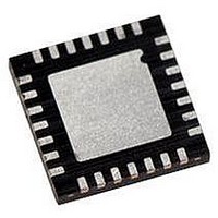
PIC18LF27J53-I/ML Microchip Technology, PIC18LF27J53-I/ML Datasheet - Page 158

PIC18LF27J53-I/ML
Manufacturer Part Number
PIC18LF27J53-I/ML
Description
IC PIC MCU 128KB FLASH 28QFN
Manufacturer
Microchip Technology
Series
PIC® XLP™ 18Fr
Datasheets
1.PIC18LF24J10-ISS.pdf
(32 pages)
2.PIC18F26J13-ISS.pdf
(496 pages)
3.PIC18F26J53-ISS.pdf
(586 pages)
4.PIC18F26J53-ISS.pdf
(12 pages)
Specifications of PIC18LF27J53-I/ML
Core Size
8-Bit
Program Memory Size
128KB (64K x 16)
Core Processor
PIC
Speed
48MHz
Connectivity
I²C, LIN, SPI, UART/USART, USB
Peripherals
Brown-out Detect/Reset, POR, PWM, WDT
Number Of I /o
22
Program Memory Type
FLASH
Ram Size
3.8K x 8
Voltage - Supply (vcc/vdd)
2 V ~ 2.75 V
Data Converters
A/D 10x10b/12b
Oscillator Type
Internal
Operating Temperature
-40°C ~ 85°C
Package / Case
*
Controller Family/series
PIC18
Cpu Speed
48MHz
Digital Ic Case Style
QFN
Supply Voltage Range
1.8V To 3.6V
Embedded Interface Type
I2C, SPI, USART
Rohs Compliant
Yes
Lead Free Status / RoHS Status
Lead free / RoHS Compliant
Eeprom Size
-
Lead Free Status / RoHS Status
Lead free / RoHS Compliant, Lead free / RoHS Compliant
Available stocks
Company
Part Number
Manufacturer
Quantity
Price
Company:
Part Number:
PIC18LF27J53-I/ML
Manufacturer:
ATMEL
Quantity:
101
- PIC18LF24J10-ISS PDF datasheet
- PIC18F26J13-ISS PDF datasheet #2
- PIC18F26J53-ISS PDF datasheet #3
- PIC18F26J53-ISS PDF datasheet #4
- Current page: 158 of 586
- Download datasheet (6Mb)
PIC18F47J53 FAMILY
10.6
Depending on the particular PIC18F47J53 family
device selected, PORTE is implemented in two
different ways.
For 44-pin devices, PORTE is a 3-bit wide port. Three
pins (RE0/AN5/PMRD, RE1/AN6/PMWR and RE2/
AN7/PMCS) are individually configurable as inputs or
outputs. These pins have Schmitt Trigger input buffers.
When selected as analog inputs, these pins will read as
‘0’s.
The corresponding Data Direction register is TRISE.
Setting a TRISE bit (= 1) will make the corresponding
PORTE pin an input (i.e., put the corresponding output
driver in a High-Impedance mode). Clearing a TRISE
bit (= 0) will make the corresponding PORTE pin an
output (i.e., put the contents of the output latch on the
selected pin).
TRISE controls the direction of the RE pins, even when
they are being used as analog inputs. The user must
make sure to keep the pins configured as inputs when
using them as analog inputs.
The Data Latch register (LATE) is also memory
mapped. Read-modify-write operations on the LATE
register read and write the latched output value for
PORTE.
DS39964B-page 158
Note:
Note:
PORTE, TRISE and LATE
Registers
PORTE is available only in 44-pin devices.
On a POR, RE<2:0> are configured as
analog inputs.
Preliminary
EXAMPLE 10-6:
Each of the PORTE pins has a weak internal pull-up. A
single control bit can turn on all the pull-ups. This is per-
formed by setting bit, REPU (TRISE<6>). The weak
pull-up is automatically turned off when the port pin is
configured as an output. The pull-ups are disabled on a
POR. The integrated weak pull-ups consist of a semi-
conductor structure similar to, but somewhat different,
from a discrete resistor. On an unloaded I/O pin, the
weak pull-ups are intended to provide logic high indica-
tion, but will not necessarily pull the pin all the way to
V
Note that the pull-ups can be used for any set of
features, similar to the pull-ups found on PORTB.
CLRF
CLRF
MOVLW
MOVWF
MOVLW
MOVWF
DD
levels.
PORTE
LATE
0Ah
ADCON1
03h
TRISE
; Initialize PORTE by
; clearing output
; data latches
; Alternate method
; to clear output
; data latches
; Configure A/D
; for digital inputs
; Value used to
; initialize data
; direction
; Set RE<0> as inputs
; RE<1> as outputs
; RE<2> as inputs
INITIALIZING PORTE
2010 Microchip Technology Inc.
Related parts for PIC18LF27J53-I/ML
Image
Part Number
Description
Manufacturer
Datasheet
Request
R

Part Number:
Description:
Manufacturer:
Microchip Technology Inc.
Datasheet:

Part Number:
Description:
Manufacturer:
Microchip Technology Inc.
Datasheet:

Part Number:
Description:
Manufacturer:
Microchip Technology Inc.
Datasheet:

Part Number:
Description:
Manufacturer:
Microchip Technology Inc.
Datasheet:

Part Number:
Description:
Manufacturer:
Microchip Technology Inc.
Datasheet:

Part Number:
Description:
Manufacturer:
Microchip Technology Inc.
Datasheet:

Part Number:
Description:
Manufacturer:
Microchip Technology Inc.
Datasheet:

Part Number:
Description:
Manufacturer:
Microchip Technology Inc.
Datasheet:


