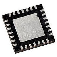
PIC18LF27J53-I/ML Microchip Technology, PIC18LF27J53-I/ML Datasheet - Page 216

PIC18LF27J53-I/ML
Manufacturer Part Number
PIC18LF27J53-I/ML
Description
IC PIC MCU 128KB FLASH 28QFN
Manufacturer
Microchip Technology
Series
PIC® XLP™ 18Fr
Datasheets
1.PIC18LF24J10-ISS.pdf
(32 pages)
2.PIC18F26J13-ISS.pdf
(496 pages)
3.PIC18F26J53-ISS.pdf
(586 pages)
4.PIC18F26J53-ISS.pdf
(12 pages)
Specifications of PIC18LF27J53-I/ML
Core Size
8-Bit
Program Memory Size
128KB (64K x 16)
Core Processor
PIC
Speed
48MHz
Connectivity
I²C, LIN, SPI, UART/USART, USB
Peripherals
Brown-out Detect/Reset, POR, PWM, WDT
Number Of I /o
22
Program Memory Type
FLASH
Ram Size
3.8K x 8
Voltage - Supply (vcc/vdd)
2 V ~ 2.75 V
Data Converters
A/D 10x10b/12b
Oscillator Type
Internal
Operating Temperature
-40°C ~ 85°C
Package / Case
*
Controller Family/series
PIC18
Cpu Speed
48MHz
Digital Ic Case Style
QFN
Supply Voltage Range
1.8V To 3.6V
Embedded Interface Type
I2C, SPI, USART
Rohs Compliant
Yes
Lead Free Status / RoHS Status
Lead free / RoHS Compliant
Eeprom Size
-
Lead Free Status / RoHS Status
Lead free / RoHS Compliant, Lead free / RoHS Compliant
Available stocks
Company
Part Number
Manufacturer
Quantity
Price
Company:
Part Number:
PIC18LF27J53-I/ML
Manufacturer:
ATMEL
Quantity:
101
- PIC18LF24J10-ISS PDF datasheet
- PIC18F26J13-ISS PDF datasheet #2
- PIC18F26J53-ISS PDF datasheet #3
- PIC18F26J53-ISS PDF datasheet #4
- Current page: 216 of 586
- Download datasheet (6Mb)
PIC18F47J53 FAMILY
13.8.2
The Timer1 gate source can be selected from one of
four different sources. Source selection is controlled by
the T1GSSx bits of the T1GCON register. The polarity
for each available source is also selectable. Polarity
selection is controlled by the T1GPOL bit of the
T1GCON register.
TABLE 13-4:
13.8.2.1
The T1G pin is one source for Timer1 gate control. It
can be used to supply an external source to the Timer1
gate circuitry.
FIGURE 13-5:
DS39964B-page 216
T1GSS<1:0>
TMR1GE
T1GPOL
T1GVAL
T1G_IN
T1GTM
Timer1
00
01
10
11
T1CKI
TIMER1 GATE SOURCE
SELECTION
T1G Pin Gate Operation
Timer1 Gate Pin
TMR2 matches PR2
Comparator 1 output
Comparator 2 output
TIMER1 GATE SOURCES
N
TIMER1 GATE TOGGLE MODE
Timer1 Gate Source
N + 1 N + 2 N + 3
Preliminary
13.8.2.2
The TMR2 register will increment until it matches the
value in the PR2 register. On the very next increment
cycle, TMR2 will be reset to 00h. When this Reset
occurs, a low-to-high pulse will automatically be
generated and internally supplied to the Timer1 gate
circuitry.
13.8.3
When Timer1 Gate Toggle mode is enabled, it is
possible to measure the full cycle length of a Timer1
gate signal, as opposed to the duration of a single level
pulse.
The Timer1 gate source is routed through a flip-flop that
changes state on every incrementing edge of the
signal. See Figure 13-5 for timing details.
The T1GVAL bit will indicate when the Toggled mode is
active and the timer is counting.
The Timer1 Gate Toggle mode is enabled by setting the
T1GTM bit of the T1GCON register. When the T1GTM
bit is cleared, the flip-flop is cleared and held clear. This
is necessary in order to control which edge is
measured.
N + 4
TIMER1 GATE TOGGLE MODE
Timer2 Match Gate Operation
N + 5 N + 6 N + 7
2010 Microchip Technology Inc.
N + 8
Related parts for PIC18LF27J53-I/ML
Image
Part Number
Description
Manufacturer
Datasheet
Request
R

Part Number:
Description:
Manufacturer:
Microchip Technology Inc.
Datasheet:

Part Number:
Description:
Manufacturer:
Microchip Technology Inc.
Datasheet:

Part Number:
Description:
Manufacturer:
Microchip Technology Inc.
Datasheet:

Part Number:
Description:
Manufacturer:
Microchip Technology Inc.
Datasheet:

Part Number:
Description:
Manufacturer:
Microchip Technology Inc.
Datasheet:

Part Number:
Description:
Manufacturer:
Microchip Technology Inc.
Datasheet:

Part Number:
Description:
Manufacturer:
Microchip Technology Inc.
Datasheet:

Part Number:
Description:
Manufacturer:
Microchip Technology Inc.
Datasheet:


