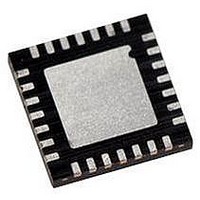
PIC18LF27J53-I/ML Microchip Technology, PIC18LF27J53-I/ML Datasheet - Page 223

PIC18LF27J53-I/ML
Manufacturer Part Number
PIC18LF27J53-I/ML
Description
IC PIC MCU 128KB FLASH 28QFN
Manufacturer
Microchip Technology
Series
PIC® XLP™ 18Fr
Datasheets
1.PIC18LF24J10-ISS.pdf
(32 pages)
2.PIC18F26J13-ISS.pdf
(496 pages)
3.PIC18F26J53-ISS.pdf
(586 pages)
4.PIC18F26J53-ISS.pdf
(12 pages)
Specifications of PIC18LF27J53-I/ML
Core Size
8-Bit
Program Memory Size
128KB (64K x 16)
Core Processor
PIC
Speed
48MHz
Connectivity
I²C, LIN, SPI, UART/USART, USB
Peripherals
Brown-out Detect/Reset, POR, PWM, WDT
Number Of I /o
22
Program Memory Type
FLASH
Ram Size
3.8K x 8
Voltage - Supply (vcc/vdd)
2 V ~ 2.75 V
Data Converters
A/D 10x10b/12b
Oscillator Type
Internal
Operating Temperature
-40°C ~ 85°C
Package / Case
*
Controller Family/series
PIC18
Cpu Speed
48MHz
Digital Ic Case Style
QFN
Supply Voltage Range
1.8V To 3.6V
Embedded Interface Type
I2C, SPI, USART
Rohs Compliant
Yes
Lead Free Status / RoHS Status
Lead free / RoHS Compliant
Eeprom Size
-
Lead Free Status / RoHS Status
Lead free / RoHS Compliant, Lead free / RoHS Compliant
Available stocks
Company
Part Number
Manufacturer
Quantity
Price
Company:
Part Number:
PIC18LF27J53-I/ML
Manufacturer:
ATMEL
Quantity:
101
- PIC18LF24J10-ISS PDF datasheet
- PIC18F26J13-ISS PDF datasheet #2
- PIC18F26J53-ISS PDF datasheet #3
- PIC18F26J53-ISS PDF datasheet #4
- Current page: 223 of 586
- Download datasheet (6Mb)
15.1
The Timer3/5 Gate Control register (TxGCON), pro-
vided in Register 14-2, is used to control the Timerx
gate.
REGISTER 15-2:
2010 Microchip Technology Inc.
bit 7
Legend:
R = Readable bit
-n = Value at POR
bit 7
bit 6
bit 5
bit 4
bit 3
bit 2
bit 1-0
Note 1:
TMRxGE
R/W-0
Timer3/5 Gate Control Register
Programming the TxGCON prior to TxCON is recommended.
TMRxGE: Timer Gate Enable bit
If TMRxON = 0:
This bit is ignored.
If TMRxON = 1:
1 = Timer counting is controlled by the Timerx gate function
0 = Timer counts regardless of the Timerx gate function
TxGPOL: Gate Polarity bit
1 = Timer gate is active-high (Timerx counts when the gate is high)
0 = Timer gate is active-low (Timerx counts when the gate is low)
TxGTM: Gate Toggle Mode bit
1 = Timer Gate Toggle mode is enabled.
0 = Timer Gate Toggle mode is disabled and toggle flip-flop is cleared
Timerx gate flip-flop toggles on every rising edge.
TxGSPM: Timer Gate Single Pulse Mode bit
1 = Timer Gate Single Pulse mode is enabled and is controlling Timerx gate
0 = Timer Gate Single Pulse mode is disabled
TxGGO/TxDONE: Timer Gate Single Pulse Acquisition Status bit
1 = Timer gate single pulse acquisition is ready, waiting for an edge
0 = Timer gate single pulse acquisition has completed or has not been started
This bit is automatically cleared when TxGSPM is cleared.
TxGVAL: Timer Gate Current State bit
Indicates the current state of the Timer gate that could be provided to TMRxH:TMRxL. Unaffected by the
Timer Gate Enable bit (TMRxGE).
TxGSS<1:0>: Timer Gate Source Select bits
11 = Comparator 2 output
10 = Comparator 1 output
01 = TMR4/6 to match PR4/6 output
00 = T3G/T5G gate input pin
TxGPOL
R/W-0
TxGCON: TIMER3/5 GATE CONTROL REGISTER
BANKED F21h)
W = Writable bit
‘1’ = Bit is set
TxGTM
R/W-0
TxGSPM
R/W-0
Preliminary
U = Unimplemented bit, read as ‘0’
‘0’ = Bit is cleared
TxGGO/TxDONE
R/W-0
PIC18F47J53 FAMILY
TxGVAL
R-x
(1)
(ACCESS F97h,
x = Bit is unknown
TxGSS1
R/W-0
DS39964B-page 223
TxGSS0
R/W-0
bit 0
Related parts for PIC18LF27J53-I/ML
Image
Part Number
Description
Manufacturer
Datasheet
Request
R

Part Number:
Description:
Manufacturer:
Microchip Technology Inc.
Datasheet:

Part Number:
Description:
Manufacturer:
Microchip Technology Inc.
Datasheet:

Part Number:
Description:
Manufacturer:
Microchip Technology Inc.
Datasheet:

Part Number:
Description:
Manufacturer:
Microchip Technology Inc.
Datasheet:

Part Number:
Description:
Manufacturer:
Microchip Technology Inc.
Datasheet:

Part Number:
Description:
Manufacturer:
Microchip Technology Inc.
Datasheet:

Part Number:
Description:
Manufacturer:
Microchip Technology Inc.
Datasheet:

Part Number:
Description:
Manufacturer:
Microchip Technology Inc.
Datasheet:


