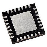
PIC18LF27J53-I/ML Microchip Technology, PIC18LF27J53-I/ML Datasheet - Page 357

PIC18LF27J53-I/ML
Manufacturer Part Number
PIC18LF27J53-I/ML
Description
IC PIC MCU 128KB FLASH 28QFN
Manufacturer
Microchip Technology
Series
PIC® XLP™ 18Fr
Datasheets
1.PIC18LF24J10-ISS.pdf
(32 pages)
2.PIC18F26J13-ISS.pdf
(496 pages)
3.PIC18F26J53-ISS.pdf
(586 pages)
4.PIC18F26J53-ISS.pdf
(12 pages)
Specifications of PIC18LF27J53-I/ML
Core Size
8-Bit
Program Memory Size
128KB (64K x 16)
Core Processor
PIC
Speed
48MHz
Connectivity
I²C, LIN, SPI, UART/USART, USB
Peripherals
Brown-out Detect/Reset, POR, PWM, WDT
Number Of I /o
22
Program Memory Type
FLASH
Ram Size
3.8K x 8
Voltage - Supply (vcc/vdd)
2 V ~ 2.75 V
Data Converters
A/D 10x10b/12b
Oscillator Type
Internal
Operating Temperature
-40°C ~ 85°C
Package / Case
*
Controller Family/series
PIC18
Cpu Speed
48MHz
Digital Ic Case Style
QFN
Supply Voltage Range
1.8V To 3.6V
Embedded Interface Type
I2C, SPI, USART
Rohs Compliant
Yes
Lead Free Status / RoHS Status
Lead free / RoHS Compliant
Eeprom Size
-
Lead Free Status / RoHS Status
Lead free / RoHS Compliant, Lead free / RoHS Compliant
Available stocks
Company
Part Number
Manufacturer
Quantity
Price
Company:
Part Number:
PIC18LF27J53-I/ML
Manufacturer:
ATMEL
Quantity:
101
- PIC18LF24J10-ISS PDF datasheet
- PIC18F26J13-ISS PDF datasheet #2
- PIC18F26J53-ISS PDF datasheet #3
- PIC18F26J53-ISS PDF datasheet #4
- Current page: 357 of 586
- Download datasheet (6Mb)
21.2.2
The receiver block diagram is displayed in Figure 21-6.
The data is received on the RXx pin and drives the data
recovery block. The data recovery block is actually a
high-speed shifter, operating at x16 times the baud
rate, whereas the main receive serial shifter operates
at the bit rate or at F
used in RS-232 systems.
To set up an Asynchronous Reception:
1.
2.
3.
4.
5.
6.
7.
8.
9.
10. If using interrupts, ensure that the GIE and PEIE
FIGURE 21-6:
2010 Microchip Technology Inc.
Initialize the SPBRGHx:SPBRGx registers for
the appropriate baud rate. Set or clear the
BRGH and BRG16 bits, as required, to achieve
the desired baud rate.
Enable the asynchronous serial port by clearing
bit, SYNC, and setting bit, SPEN.
If interrupts are desired, set enable bit, RCxIE.
If 9-bit reception is desired, set bit, RX9.
Enable the reception by setting bit, CREN.
Flag bit, RCxIF, will be set when reception is
complete and an interrupt will be generated if
enable bit, RCxIE, was set.
Read the RCSTAx register to get the ninth bit (if
enabled) and determine if any error occurred
during reception.
Read the 8-bit received data by reading the
RCREGx register.
If any error occurred, clear the error by clearing
enable bit, CREN.
bits in the INTCON register (INTCON<7:6>) are
set.
EUSART ASYNCHRONOUS
RECEIVER
RXx
BRG16
OSC
EUSARTx RECEIVE BLOCK DIAGRAM
SPBRGHx
. This mode would typically be
Baud Rate Generator
x64 Baud Rate CLK
and Control
Pin Buffer
SPEN
SPBRGx
Recovery
Interrupt
Preliminary
64
16
4
Data
or
or
CREN
PIC18F47J53 FAMILY
21.2.3
This mode would typically be used in RS-485 systems.
To set up an Asynchronous Reception with Address
Detect Enable:
1.
2.
3.
4.
5.
6.
7.
8.
9.
10. If any error occurred, clear the CREN bit.
11. If the device has been addressed, clear the
RX9
Initialize the SPBRGHx:SPBRGx registers for
the appropriate baud rate. Set or clear the
BRGH and BRG16 bits, as required, to achieve
the desired baud rate.
Enable the asynchronous serial port by clearing
the SYNC bit and setting the SPEN bit.
If interrupts are required, set the RCEN bit and
select the desired priority level with the RCxIP bit.
Set the RX9 bit to enable 9-bit reception.
Set the ADDEN bit to enable address detect.
Enable reception by setting the CREN bit.
The RCxIF bit will be set when reception is
complete. The interrupt will be Acknowledged if
the RCxIE and GIE bits are set.
Read the RCSTAx register to determine if any
error occurred during reception, as well as read
bit 9 of data (if applicable).
Read RCREGx to determine if the device is
being addressed.
ADDEN bit to allow all received data into the
receive buffer and interrupt the CPU.
Stop
MSb
RCxIF
RCxIE
RX9D
SETTING UP 9-BIT MODE WITH
ADDRESS DETECT
(8)
OERR
7
RSR Register
RCREGx Register
8
Data Bus
1
FERR
0
DS39964B-page 357
LSb
Start
FIFO
Related parts for PIC18LF27J53-I/ML
Image
Part Number
Description
Manufacturer
Datasheet
Request
R

Part Number:
Description:
Manufacturer:
Microchip Technology Inc.
Datasheet:

Part Number:
Description:
Manufacturer:
Microchip Technology Inc.
Datasheet:

Part Number:
Description:
Manufacturer:
Microchip Technology Inc.
Datasheet:

Part Number:
Description:
Manufacturer:
Microchip Technology Inc.
Datasheet:

Part Number:
Description:
Manufacturer:
Microchip Technology Inc.
Datasheet:

Part Number:
Description:
Manufacturer:
Microchip Technology Inc.
Datasheet:

Part Number:
Description:
Manufacturer:
Microchip Technology Inc.
Datasheet:

Part Number:
Description:
Manufacturer:
Microchip Technology Inc.
Datasheet:


