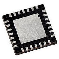
PIC18LF27J53-I/ML Microchip Technology, PIC18LF27J53-I/ML Datasheet - Page 257

PIC18LF27J53-I/ML
Manufacturer Part Number
PIC18LF27J53-I/ML
Description
IC PIC MCU 128KB FLASH 28QFN
Manufacturer
Microchip Technology
Series
PIC® XLP™ 18Fr
Datasheets
1.PIC18LF24J10-ISS.pdf
(32 pages)
2.PIC18F26J13-ISS.pdf
(496 pages)
3.PIC18F26J53-ISS.pdf
(586 pages)
4.PIC18F26J53-ISS.pdf
(12 pages)
Specifications of PIC18LF27J53-I/ML
Core Size
8-Bit
Program Memory Size
128KB (64K x 16)
Core Processor
PIC
Speed
48MHz
Connectivity
I²C, LIN, SPI, UART/USART, USB
Peripherals
Brown-out Detect/Reset, POR, PWM, WDT
Number Of I /o
22
Program Memory Type
FLASH
Ram Size
3.8K x 8
Voltage - Supply (vcc/vdd)
2 V ~ 2.75 V
Data Converters
A/D 10x10b/12b
Oscillator Type
Internal
Operating Temperature
-40°C ~ 85°C
Package / Case
*
Controller Family/series
PIC18
Cpu Speed
48MHz
Digital Ic Case Style
QFN
Supply Voltage Range
1.8V To 3.6V
Embedded Interface Type
I2C, SPI, USART
Rohs Compliant
Yes
Lead Free Status / RoHS Status
Lead free / RoHS Compliant
Eeprom Size
-
Lead Free Status / RoHS Status
Lead free / RoHS Compliant, Lead free / RoHS Compliant
Available stocks
Company
Part Number
Manufacturer
Quantity
Price
Company:
Part Number:
PIC18LF27J53-I/ML
Manufacturer:
ATMEL
Quantity:
101
- PIC18LF24J10-ISS PDF datasheet
- PIC18F26J13-ISS PDF datasheet #2
- PIC18F26J53-ISS PDF datasheet #3
- PIC18F26J53-ISS PDF datasheet #4
- Current page: 257 of 586
- Download datasheet (6Mb)
18.0
PIC18F47J53 family devices have seven CCP
(Capture/Compare/PWM) modules, designated CCP4
through CCP10. All the modules implement standard
Capture, Compare and Pulse-Width Modulation (PWM)
modes.
REGISTER 18-1:
2010 Microchip Technology Inc.
bit 7
Legend:
R = Readable bit
-n = Value at POR
bit 7-6
bit 5-4
bit 3-0
Note 1:
Note:
U-0
—
CAPTURE/COMPARE/PWM
(CCP) MODULES
CCPxM<3:0> = 1011 will only reset timer and not start A/D conversion on CCPx match.
Throughout this section, generic references
are used for register and bit names that are
the same – except for an ‘x’ variable that
indicates the item’s association with the
specific CCP module. For example, the con-
trol register is named CCPxCON and refers
to CCP4CON through CCP10CON.
Unimplemented: Read as ‘0’
DCxB<1:0>: PWM Duty Cycle bit 1 and bit 0 for CCPx Module
Capture mode:
Unused.
Compare mode:
Unused.
PWM mode:
These bits are the two Least Significant bits (bit 1 and bit 0) of the 10-bit PWM duty cycle. The eight Most
Significant bits (DCxB<9:2>) of the duty cycle are found in CCPRxL.
CCPxM<3:0>: CCPx Module Mode Select bits
0000 = Capture/Compare/PWM disabled (resets CCPx module)
0001 = Reserved
0010 = Compare mode, toggle output on match (CCPxIF bit is set)
0011 = Reserved
0100 = Capture mode: every falling edge
0101 = Capture mode: every rising edge
0110 = Capture mode: every 4th rising edge
0111 = Capture mode: every 16th rising edge
1000 = Compare mode: initialize CCPx pin low; on compare match, force CCPx pin high (CCPxIF bit is set)
1001 = Compare mode: initialize CCPx pin high; on compare match, force CCPx pin low (CCPxIF bit is set)
1010 = Compare mode: generate software interrupt on compare match (CCPxIF bit is set, CCPx pin
1011 = Compare mode: Special Event Trigger; reset timer on CCPx match (CCPxIF bit is set)
11xx = PWM mode
U-0
—
CCPxCON: CCP4-10 CONTROL REGISTER (4, BANKED F12h; 5, F0Fh; 6, F0Ch;
7, F09h; 8, F06h; 9, F03h; 10, F00h)
reflects I/O state)
W = Writable bit
‘1’ = Bit is set
DCxB1
R/W-0
DCxB0
R/W-0
Preliminary
U = Unimplemented bit, read as ‘0’
‘0’ = Bit is cleared
CCPxM3
PIC18F47J53 FAMILY
R/W-0
Each CCP module contains a 16-bit register that can
operate as a 16-bit Capture register, a 16-bit Compare
register or a PWM Master/Slave Duty Cycle register.
For the sake of clarity, all CCP module operation in the
following sections is described with respect to CCP4,
but is equally applicable to CCP5 through CCP10.
CCPxM2
R/W-0
x = Bit is unknown
CCPxM1
R/W-0
DS39964B-page 257
CCPxM0
R/W-0
bit 0
Related parts for PIC18LF27J53-I/ML
Image
Part Number
Description
Manufacturer
Datasheet
Request
R

Part Number:
Description:
Manufacturer:
Microchip Technology Inc.
Datasheet:

Part Number:
Description:
Manufacturer:
Microchip Technology Inc.
Datasheet:

Part Number:
Description:
Manufacturer:
Microchip Technology Inc.
Datasheet:

Part Number:
Description:
Manufacturer:
Microchip Technology Inc.
Datasheet:

Part Number:
Description:
Manufacturer:
Microchip Technology Inc.
Datasheet:

Part Number:
Description:
Manufacturer:
Microchip Technology Inc.
Datasheet:

Part Number:
Description:
Manufacturer:
Microchip Technology Inc.
Datasheet:

Part Number:
Description:
Manufacturer:
Microchip Technology Inc.
Datasheet:


