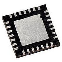
PIC18LF27J53-I/ML Microchip Technology, PIC18LF27J53-I/ML Datasheet - Page 296

PIC18LF27J53-I/ML
Manufacturer Part Number
PIC18LF27J53-I/ML
Description
IC PIC MCU 128KB FLASH 28QFN
Manufacturer
Microchip Technology
Series
PIC® XLP™ 18Fr
Datasheets
1.PIC18LF24J10-ISS.pdf
(32 pages)
2.PIC18F26J13-ISS.pdf
(496 pages)
3.PIC18F26J53-ISS.pdf
(586 pages)
4.PIC18F26J53-ISS.pdf
(12 pages)
Specifications of PIC18LF27J53-I/ML
Core Size
8-Bit
Program Memory Size
128KB (64K x 16)
Core Processor
PIC
Speed
48MHz
Connectivity
I²C, LIN, SPI, UART/USART, USB
Peripherals
Brown-out Detect/Reset, POR, PWM, WDT
Number Of I /o
22
Program Memory Type
FLASH
Ram Size
3.8K x 8
Voltage - Supply (vcc/vdd)
2 V ~ 2.75 V
Data Converters
A/D 10x10b/12b
Oscillator Type
Internal
Operating Temperature
-40°C ~ 85°C
Package / Case
*
Controller Family/series
PIC18
Cpu Speed
48MHz
Digital Ic Case Style
QFN
Supply Voltage Range
1.8V To 3.6V
Embedded Interface Type
I2C, SPI, USART
Rohs Compliant
Yes
Lead Free Status / RoHS Status
Lead free / RoHS Compliant
Eeprom Size
-
Lead Free Status / RoHS Status
Lead free / RoHS Compliant, Lead free / RoHS Compliant
Available stocks
Company
Part Number
Manufacturer
Quantity
Price
Company:
Part Number:
PIC18LF27J53-I/ML
Manufacturer:
ATMEL
Quantity:
101
- PIC18LF24J10-ISS PDF datasheet
- PIC18F26J13-ISS PDF datasheet #2
- PIC18F26J53-ISS PDF datasheet #3
- PIC18F26J53-ISS PDF datasheet #4
- Current page: 296 of 586
- Download datasheet (6Mb)
PIC18F47J53 FAMILY
20.3.4
To enable the serial port, MSSP Enable bit, SSPEN
(SSPxCON1<5>), must be set. To reset or reconfigure
SPI mode, clear the SSPEN bit, re-initialize the
SSPxCON1 registers and then set the SSPEN bit. This
configures the SDIx, SDOx, SCKx and SSx pins as
serial port pins. For the pins to behave as the serial port
function, the appropriate TRISx bits, PCFGx bits and
Peripheral Pin Select registers (if using MSSP2) should
be correctly initialized prior to setting the SSPEN bit.
A typical SPI serial port initialization process follows:
• Initialize the ODCON3 register (optional
• Initialize the remappable pin functions (if using
• Initialize the SCKx/LAT value to the desired Idle
• Initialize the SCKx/PCFGx bit (if in Slave mode
• Initialize the SCKx/TRIS bit as output (Master
• Initialize the SDIx/PCFGx bit (if SDIx is
• Initialize the SDIx/TRIS bit
• Initialize the SSx/PCFG bit (if in Slave mode and
• Initialize the SSx/TRIS bit (Slave modes)
• Initialize the SDOx/TRIS bit
• Initialize the SSPxSTAT register
• Initialize the SSPxCON1 register
• Set the SSPEN bit to enable the module
FIGURE 20-2:
DS39964B-page 296
open-drain output control)
MSSP2, see Section 10.7 “Peripheral Pin
Select (PPS)”)
SCKx level (if master device)
and multiplexed with the ANx function)
mode) or input (Slave mode)
multiplexed with the ANx function)
multiplexed the with ANx function)
ENABLING SPI I/O
SPI Master SSPM<3:0> = 00xxb
MSb
PROCESSOR 1
Serial Input Buffer
SPI MASTER/SLAVE CONNECTION
Shift Register
(SSPxBUF)
(SSPxSR)
LSb
SDOx
SCKx
SDIx
Preliminary
Serial Clock
initiates the data transfer by sending the SCKx signal.
Any MSSP1 serial port function that is not desired may
be overridden by programming the corresponding Data
Direction (TRIS) register to the opposite value. If
individual MSSP2 serial port functions will not be used,
they may be left unmapped.
20.3.5
Figure 20-2 illustrates a typical connection between two
microcontrollers. The master controller (Processor 1)
Data is shifted out of both shift registers on their pro-
grammed clock edge and latched on the opposite edge
of the clock. Both processors should be programmed to
the same Clock Polarity (CKP), then both controllers
would send and receive data at the same time. Whether
the data is meaningful (or dummy data) depends on the
application software. This leads to three scenarios for
data transmission:
• Master sends valid data–Slave sends dummy
• Master sends valid data–Slave sends valid data
• Master sends dummy data–Slave sends valid data
Note:
data
SDOx
SCKx
SDIx
When MSSP2 is used in SPI Master
mode, the SCK2 function must be config-
ured as both an output and an input in the
PPS module. SCK2 must be initialized as
an output pin (by writing 0x0A to one of the
RPORx registers). Additionally, SCK2IN
must also be mapped to the same pin by
initializing the RPINR22 register. Failure to
initialize SCK2/SCK2IN as both output
and input will prevent the module from
receiving data on the SDI2 pin, as the
module uses the SCK2IN signal to latch
the received data.
TYPICAL CONNECTION
SPI Slave SSPM<3:0> = 010xb
MSb
Serial Input Buffer
Shift Register
PROCESSOR 2
(SSPxBUF)
(SSPxSR)
2010 Microchip Technology Inc.
LSb
Related parts for PIC18LF27J53-I/ML
Image
Part Number
Description
Manufacturer
Datasheet
Request
R

Part Number:
Description:
Manufacturer:
Microchip Technology Inc.
Datasheet:

Part Number:
Description:
Manufacturer:
Microchip Technology Inc.
Datasheet:

Part Number:
Description:
Manufacturer:
Microchip Technology Inc.
Datasheet:

Part Number:
Description:
Manufacturer:
Microchip Technology Inc.
Datasheet:

Part Number:
Description:
Manufacturer:
Microchip Technology Inc.
Datasheet:

Part Number:
Description:
Manufacturer:
Microchip Technology Inc.
Datasheet:

Part Number:
Description:
Manufacturer:
Microchip Technology Inc.
Datasheet:

Part Number:
Description:
Manufacturer:
Microchip Technology Inc.
Datasheet:


