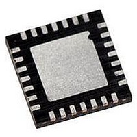
PIC18LF27J53-I/ML Microchip Technology, PIC18LF27J53-I/ML Datasheet - Page 318

PIC18LF27J53-I/ML
Manufacturer Part Number
PIC18LF27J53-I/ML
Description
IC PIC MCU 128KB FLASH 28QFN
Manufacturer
Microchip Technology
Series
PIC® XLP™ 18Fr
Datasheets
1.PIC18LF24J10-ISS.pdf
(32 pages)
2.PIC18F26J13-ISS.pdf
(496 pages)
3.PIC18F26J53-ISS.pdf
(586 pages)
4.PIC18F26J53-ISS.pdf
(12 pages)
Specifications of PIC18LF27J53-I/ML
Core Size
8-Bit
Program Memory Size
128KB (64K x 16)
Core Processor
PIC
Speed
48MHz
Connectivity
I²C, LIN, SPI, UART/USART, USB
Peripherals
Brown-out Detect/Reset, POR, PWM, WDT
Number Of I /o
22
Program Memory Type
FLASH
Ram Size
3.8K x 8
Voltage - Supply (vcc/vdd)
2 V ~ 2.75 V
Data Converters
A/D 10x10b/12b
Oscillator Type
Internal
Operating Temperature
-40°C ~ 85°C
Package / Case
*
Controller Family/series
PIC18
Cpu Speed
48MHz
Digital Ic Case Style
QFN
Supply Voltage Range
1.8V To 3.6V
Embedded Interface Type
I2C, SPI, USART
Rohs Compliant
Yes
Lead Free Status / RoHS Status
Lead free / RoHS Compliant
Eeprom Size
-
Lead Free Status / RoHS Status
Lead free / RoHS Compliant, Lead free / RoHS Compliant
Available stocks
Company
Part Number
Manufacturer
Quantity
Price
Company:
Part Number:
PIC18LF27J53-I/ML
Manufacturer:
ATMEL
Quantity:
101
- PIC18LF24J10-ISS PDF datasheet
- PIC18F26J13-ISS PDF datasheet #2
- PIC18F26J53-ISS PDF datasheet #3
- PIC18F26J53-ISS PDF datasheet #4
- Current page: 318 of 586
- Download datasheet (6Mb)
PIC18F47J53 FAMILY
20.5.3.5
When the R/W bit of the address byte is clear and an
address match occurs, the R/W bit of the SSPxSTAT
register is cleared. The received address is loaded into
the SSPxBUF register and the SDAx line is held low
(ACK).
When the address byte overflow condition exists, then
the no Acknowledge (ACK) pulse is given. An overflow
condition is defined as either bit, BF (SSPxSTAT<0>),
is set or bit, SSPOV (SSPxCON1<6>), is set.
An MSSP interrupt is generated for each data transfer
byte. The interrupt flag bit, SSPxIF, must be cleared in
software. The SSPxSTAT register is used to determine
the status of the byte.
If SEN is enabled (SSPxCON2<0> = 1), SCLx will be
held low (clock stretch) following each data transfer.
The clock must be released by setting bit, CKP
(SSPxCON1<4>).
Stretching” for more details.
DS39964B-page 318
Reception
See
Section 20.5.4
“Clock
Preliminary
20.5.3.6
When the R/W bit of the incoming address byte is set
and an address match occurs, the R/W bit of the
SSPxSTAT register is set. The received address is
loaded into the SSPxBUF register. The ACK pulse will
be sent on the ninth bit and pin, SCLx, is held low
regardless of SEN (see Section 20.5.4 “Clock
Stretching” for more details). By stretching the clock,
the master will be unable to assert another clock pulse
until the slave is done preparing the transmit data. The
transmit data must be loaded into the SSPxBUF regis-
ter, which also loads the SSPxSR register. Then, the
SCLx pin should be enabled by setting bit, CKP
(SSPxCON1<4>). The eight data bits are shifted out on
the falling edge of the SCLx input. This ensures that the
SDAx signal is valid during the SCLx high time
(Figure 20-10).
The ACK pulse from the master-receiver is latched on
the rising edge of the ninth SCLx input pulse. If the
SDAx line is high (not ACK), then the data transfer is
complete. In this case, when the ACK is latched by the
slave, the slave logic is reset (resets the SSPxSTAT
register) and the slave monitors for another occurrence
of the Start bit. If the SDAx line was low (ACK), the next
transmit data must be loaded into the SSPxBUF
register. Again, the SCLx pin must be enabled by
setting bit, CKP.
An MSSP interrupt is generated for each data transfer
byte. The SSPxIF bit must be cleared in software and
the SSPxSTAT register is used to determine the status
of the byte. The SSPxIF bit is set on the falling edge of
the ninth clock pulse.
Transmission
2010 Microchip Technology Inc.
Related parts for PIC18LF27J53-I/ML
Image
Part Number
Description
Manufacturer
Datasheet
Request
R

Part Number:
Description:
Manufacturer:
Microchip Technology Inc.
Datasheet:

Part Number:
Description:
Manufacturer:
Microchip Technology Inc.
Datasheet:

Part Number:
Description:
Manufacturer:
Microchip Technology Inc.
Datasheet:

Part Number:
Description:
Manufacturer:
Microchip Technology Inc.
Datasheet:

Part Number:
Description:
Manufacturer:
Microchip Technology Inc.
Datasheet:

Part Number:
Description:
Manufacturer:
Microchip Technology Inc.
Datasheet:

Part Number:
Description:
Manufacturer:
Microchip Technology Inc.
Datasheet:

Part Number:
Description:
Manufacturer:
Microchip Technology Inc.
Datasheet:


