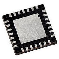
PIC18LF27J53-I/ML Microchip Technology, PIC18LF27J53-I/ML Datasheet - Page 304

PIC18LF27J53-I/ML
Manufacturer Part Number
PIC18LF27J53-I/ML
Description
IC PIC MCU 128KB FLASH 28QFN
Manufacturer
Microchip Technology
Series
PIC® XLP™ 18Fr
Datasheets
1.PIC18LF24J10-ISS.pdf
(32 pages)
2.PIC18F26J13-ISS.pdf
(496 pages)
3.PIC18F26J53-ISS.pdf
(586 pages)
4.PIC18F26J53-ISS.pdf
(12 pages)
Specifications of PIC18LF27J53-I/ML
Core Size
8-Bit
Program Memory Size
128KB (64K x 16)
Core Processor
PIC
Speed
48MHz
Connectivity
I²C, LIN, SPI, UART/USART, USB
Peripherals
Brown-out Detect/Reset, POR, PWM, WDT
Number Of I /o
22
Program Memory Type
FLASH
Ram Size
3.8K x 8
Voltage - Supply (vcc/vdd)
2 V ~ 2.75 V
Data Converters
A/D 10x10b/12b
Oscillator Type
Internal
Operating Temperature
-40°C ~ 85°C
Package / Case
*
Controller Family/series
PIC18
Cpu Speed
48MHz
Digital Ic Case Style
QFN
Supply Voltage Range
1.8V To 3.6V
Embedded Interface Type
I2C, SPI, USART
Rohs Compliant
Yes
Lead Free Status / RoHS Status
Lead free / RoHS Compliant
Eeprom Size
-
Lead Free Status / RoHS Status
Lead free / RoHS Compliant, Lead free / RoHS Compliant
Available stocks
Company
Part Number
Manufacturer
Quantity
Price
Company:
Part Number:
PIC18LF27J53-I/ML
Manufacturer:
ATMEL
Quantity:
101
- PIC18LF24J10-ISS PDF datasheet
- PIC18F26J13-ISS PDF datasheet #2
- PIC18F26J53-ISS PDF datasheet #3
- PIC18F26J53-ISS PDF datasheet #4
- Current page: 304 of 586
- Download datasheet (6Mb)
PIC18F47J53 FAMILY
REGISTER 20-3:
DS39964B-page 304
bit 7
Legend:
R = Readable bit
-n = Value at POR
bit 7-6
bit 5
bit 4
bit 3-2
bit 1
bit 0
SSCON1
R/W-0
SSCON<1:0>: SSDMA Output Control bits (Master modes only)
11 = SSDMA is asserted for the duration of 4 bytes; DLYINTEN is always reset low
01 = SSDMA is asserted for the duration of 2 bytes; DLYINTEN is always reset low
10 = SSDMA is asserted for the duration of 1 byte; DLYINTEN is always reset low
00 = SSDMA is not controlled by the DMA module; DLYINTEN bit is software programmable
TXINC: Transmit Address Increment Enable bit
Allows the transmit address to increment as the transfer progresses.
1 = The transmit address is to be incremented from the initial value of TXADDR<11:0>
0 = The transmit address is always set to the initial value of TXADDR<11:0>
RXINC: Receive Address Increment Enable bit
Allows the receive address to increment as the transfer progresses.
1 = The received address is to be incremented from the intial value of RXADDR<11:0>
0 = The received address is always set to the initial value of RXADDR<11:0>
DUPLEX<1:0>: Transmit/Receive Operating Mode Select bits
10 = SPI DMA operates in Full-Duplex mode, data is simultaneously transmitted and received
01 = DMA operates in Half-Duplex mode, data is transmitted only
00 = DMA operates in Half-Duplex mode, data is received only
DLYINTEN: Delay Interrupt Enable bit
Enables the interrupt to be invoked after the number of T
elapsed from the latest completed transfer.
1 = The interrupt is enabled, SSCON<1:0> must be set to ‘00’
0 = The interrupt is disabled
DMAEN: DMA Operation Start/Stop bit
This bit is set by the users’ software to start the DMA operation. It is reset back to zero by the DMA
engine when the DMA operation is completed or aborted.
1 = DMA is in session
0 = DMA is not in session
SSCON0
R/W-0
DMACON1: DMA CONTROL REGISTER 1 (ACCESS F88h)
W = Writable bit
‘1’ = Bit is set
TXINC
R/W-0
RXINC
R/W-0
Preliminary
U = Unimplemented bit, read as ‘0’
‘0’ = Bit is cleared
DUPLEX1
R/W-0
CY
DUPLEX0
R/W-0
cycles specified in DLYCYC<2:0> has
2010 Microchip Technology Inc.
x = Bit is unknown
DLYINTEN
R/W-0
DMAEN
R/W-0
bit 0
Related parts for PIC18LF27J53-I/ML
Image
Part Number
Description
Manufacturer
Datasheet
Request
R

Part Number:
Description:
Manufacturer:
Microchip Technology Inc.
Datasheet:

Part Number:
Description:
Manufacturer:
Microchip Technology Inc.
Datasheet:

Part Number:
Description:
Manufacturer:
Microchip Technology Inc.
Datasheet:

Part Number:
Description:
Manufacturer:
Microchip Technology Inc.
Datasheet:

Part Number:
Description:
Manufacturer:
Microchip Technology Inc.
Datasheet:

Part Number:
Description:
Manufacturer:
Microchip Technology Inc.
Datasheet:

Part Number:
Description:
Manufacturer:
Microchip Technology Inc.
Datasheet:

Part Number:
Description:
Manufacturer:
Microchip Technology Inc.
Datasheet:


