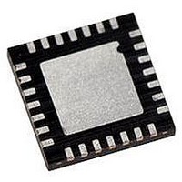
PIC18LF27J53-I/ML Microchip Technology, PIC18LF27J53-I/ML Datasheet - Page 472

PIC18LF27J53-I/ML
Manufacturer Part Number
PIC18LF27J53-I/ML
Description
IC PIC MCU 128KB FLASH 28QFN
Manufacturer
Microchip Technology
Series
PIC® XLP™ 18Fr
Datasheets
1.PIC18LF24J10-ISS.pdf
(32 pages)
2.PIC18F26J13-ISS.pdf
(496 pages)
3.PIC18F26J53-ISS.pdf
(586 pages)
4.PIC18F26J53-ISS.pdf
(12 pages)
Specifications of PIC18LF27J53-I/ML
Core Size
8-Bit
Program Memory Size
128KB (64K x 16)
Core Processor
PIC
Speed
48MHz
Connectivity
I²C, LIN, SPI, UART/USART, USB
Peripherals
Brown-out Detect/Reset, POR, PWM, WDT
Number Of I /o
22
Program Memory Type
FLASH
Ram Size
3.8K x 8
Voltage - Supply (vcc/vdd)
2 V ~ 2.75 V
Data Converters
A/D 10x10b/12b
Oscillator Type
Internal
Operating Temperature
-40°C ~ 85°C
Package / Case
*
Controller Family/series
PIC18
Cpu Speed
48MHz
Digital Ic Case Style
QFN
Supply Voltage Range
1.8V To 3.6V
Embedded Interface Type
I2C, SPI, USART
Rohs Compliant
Yes
Lead Free Status / RoHS Status
Lead free / RoHS Compliant
Eeprom Size
-
Lead Free Status / RoHS Status
Lead free / RoHS Compliant, Lead free / RoHS Compliant
Available stocks
Company
Part Number
Manufacturer
Quantity
Price
Company:
Part Number:
PIC18LF27J53-I/ML
Manufacturer:
ATMEL
Quantity:
101
- PIC18LF24J10-ISS PDF datasheet
- PIC18F26J13-ISS PDF datasheet #2
- PIC18F26J53-ISS PDF datasheet #3
- PIC18F26J53-ISS PDF datasheet #4
- Current page: 472 of 586
- Download datasheet (6Mb)
PIC18F47J53 FAMILY
BTFSC
Syntax:
Operands:
Operation:
Status Affected:
Encoding:
Description:
Words:
Cycles:
Example:
DS39964B-page 472
Q Cycle Activity:
If skip:
If skip and followed by 2-word instruction:
Before Instruction
After Instruction
operation
operation
operation
Decode
PC
If FLAG<1>
If FLAG<1>
No
No
No
Q1
Q1
Q1
PC
PC
Bit Test File, Skip if Clear
BTFSC f, b {,a}
0 f 255
0 b 7
a [0,1]
skip if (f<b>) = 0
None
If bit ‘b’ in register ‘f’ is ‘0’, then the next
instruction is skipped. If bit ‘b’ is ‘0’, then
the next instruction fetched during the
current instruction execution is discarded
and a NOP is executed instead, making
this a two-cycle instruction.
If ‘a’ is ‘0’, the Access Bank is selected. If
‘a’ is ‘1’, the BSR is used to select the
GPR bank (default).
If ‘a’ is ‘0’ and the extended instruction set
is enabled, this instruction operates in
Indexed Literal Offset Addressing mode
whenever f 95 (5Fh). See
Section 29.2.3 “Byte-Oriented and
Bit-Oriented Instructions in Indexed
Literal Offset Mode” for details.
1
1(2)
Note: 3 cycles if skip and followed
register ‘f’
HERE
FALSE
TRUE
operation
operation
operation
Read
1011
No
No
No
=
=
=
=
=
Q2
Q2
Q2
by a 2-word instruction.
address (HERE)
0;
address (TRUE)
1;
address (FALSE)
BTFSC
:
:
bbba
operation
operation
operation
Process
Data
No
No
No
Q3
Q3
Q3
FLAG, 1, 0
ffff
operation
operation
operation
operation
No
No
No
No
Q4
Q4
Q4
ffff
Preliminary
BTFSS
Syntax:
Operands:
Operation:
Status Affected:
Encoding:
Description:
Words:
Cycles:
Example:
Q Cycle Activity:
If skip:
If skip and followed by 2-word instruction:
Before Instruction
After Instruction
operation
operation
operation
Decode
PC
If FLAG<1>
If FLAG<1>
No
No
No
Q1
Q1
Q1
PC
PC
Bit Test File, Skip if Set
BTFSS f, b {,a}
0 f 255
0 b < 7
a [0,1]
skip if (f<b>) = 1
None
If bit ‘b’ in register ‘f’ is ‘1’, then the next
instruction is skipped. If bit ‘b’ is ‘1’, then
the next instruction fetched during the
current instruction execution is discarded
and a NOP is executed instead, making
this a two-cycle instruction.
If ‘a’ is ‘0’, the Access Bank is selected. If
‘a’ is ‘1’, the BSR is used to select the
GPR bank (default).
If ‘a’ is ‘0’ and the extended instruction
set is enabled, this instruction operates in
Indexed Literal Offset Addressing mode
whenever f 95 (5Fh). See
Section 29.2.3 “Byte-Oriented and
Bit-Oriented Instructions in Indexed
Literal Offset Mode” for details.
1
1(2)
Note:
register ‘f’
HERE
FALSE
TRUE
operation
operation
operation
Read
1010
No
No
No
=
=
=
=
=
Q2
Q2
Q2
2010 Microchip Technology Inc.
address (HERE)
0;
address (FALSE)
1;
address (TRUE)
3 cycles if skip and followed
by a 2-word instruction.
BTFSS
:
:
bbba
operation
operation
operation
Process
Data
No
No
No
Q3
Q3
Q3
FLAG, 1, 0
ffff
operation
operation
operation
operation
No
No
No
No
Q4
Q4
Q4
ffff
Related parts for PIC18LF27J53-I/ML
Image
Part Number
Description
Manufacturer
Datasheet
Request
R

Part Number:
Description:
Manufacturer:
Microchip Technology Inc.
Datasheet:

Part Number:
Description:
Manufacturer:
Microchip Technology Inc.
Datasheet:

Part Number:
Description:
Manufacturer:
Microchip Technology Inc.
Datasheet:

Part Number:
Description:
Manufacturer:
Microchip Technology Inc.
Datasheet:

Part Number:
Description:
Manufacturer:
Microchip Technology Inc.
Datasheet:

Part Number:
Description:
Manufacturer:
Microchip Technology Inc.
Datasheet:

Part Number:
Description:
Manufacturer:
Microchip Technology Inc.
Datasheet:

Part Number:
Description:
Manufacturer:
Microchip Technology Inc.
Datasheet:


