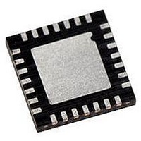
PIC18LF27J53-I/ML Microchip Technology, PIC18LF27J53-I/ML Datasheet - Page 443

PIC18LF27J53-I/ML
Manufacturer Part Number
PIC18LF27J53-I/ML
Description
IC PIC MCU 128KB FLASH 28QFN
Manufacturer
Microchip Technology
Series
PIC® XLP™ 18Fr
Datasheets
1.PIC18LF24J10-ISS.pdf
(32 pages)
2.PIC18F26J13-ISS.pdf
(496 pages)
3.PIC18F26J53-ISS.pdf
(586 pages)
4.PIC18F26J53-ISS.pdf
(12 pages)
Specifications of PIC18LF27J53-I/ML
Core Size
8-Bit
Program Memory Size
128KB (64K x 16)
Core Processor
PIC
Speed
48MHz
Connectivity
I²C, LIN, SPI, UART/USART, USB
Peripherals
Brown-out Detect/Reset, POR, PWM, WDT
Number Of I /o
22
Program Memory Type
FLASH
Ram Size
3.8K x 8
Voltage - Supply (vcc/vdd)
2 V ~ 2.75 V
Data Converters
A/D 10x10b/12b
Oscillator Type
Internal
Operating Temperature
-40°C ~ 85°C
Package / Case
*
Controller Family/series
PIC18
Cpu Speed
48MHz
Digital Ic Case Style
QFN
Supply Voltage Range
1.8V To 3.6V
Embedded Interface Type
I2C, SPI, USART
Rohs Compliant
Yes
Lead Free Status / RoHS Status
Lead free / RoHS Compliant
Eeprom Size
-
Lead Free Status / RoHS Status
Lead free / RoHS Compliant, Lead free / RoHS Compliant
Available stocks
Company
Part Number
Manufacturer
Quantity
Price
Company:
Part Number:
PIC18LF27J53-I/ML
Manufacturer:
ATMEL
Quantity:
101
- PIC18LF24J10-ISS PDF datasheet
- PIC18F26J13-ISS PDF datasheet #2
- PIC18F26J53-ISS PDF datasheet #3
- PIC18F26J53-ISS PDF datasheet #4
- Current page: 443 of 586
- Download datasheet (6Mb)
REGISTER 28-1:
2010 Microchip Technology Inc.
bit 7
Legend:
R = Readable bit
-n = Value at POR
bit 7
bit 6
bit 5
bit 4
bit 3-1
bit 0
R/WO-1
DEBUG
DEBUG: Background Debugger Enable bit
1 = Background debugger is disabled; RB6 and RB7 configured as general purpose I/O pins
0 = Background debugger is enabled; RB6 and RB7 are dedicated to In-Circuit Debug
XINST: Extended Instruction Set Enable bit
1 = Instruction set extension and Indexed Addressing mode are enabled
0 = Instruction set extension and Indexed Addressing mode are disabled
STVREN: Stack Overflow/Underflow Reset Enable bit
1 = Reset on stack overflow/underflow is enabled
0 = Reset on stack overflow/underflow is disabled
CFGPLLEN: PLL Enable bit
1 = 96 MHz PLL is disabled
0 = 96 MHz PLL is enabled
PLLDIV<2:0>: Oscillator Selection bits
Divider must be selected to provide a 4 MHz input into the 96 MHz PLL.
111 = No divide – oscillator used directly (4 MHz input)
110 = Oscillator divided by 2 (8 MHz input)
101 = Oscillator divided by 3 (12 MHz input)
100 = Oscillator divided by 4 (16 MHz input)
011 = Oscillator divided by 5 (20 MHz input)
010 = Oscillator divided by 6 (24 MHz input)
001 = Oscillator divided by 10 (40 MHz input)
000 = Oscillator divided by 12 (48 MHz input)
WDTEN: Watchdog Timer Enable bit
1 = WDT is enabled
0 = WDT is disabled (control is placed on the SWDTEN bit)
R/WO-1
XINST
CONFIG1L: CONFIGURATION REGISTER 1 LOW (BYTE ADDRESS 300000h)
WO = Write-Once bit
‘1’ = Bit is set
STVREN
R/WO-1
CFGPLLEN
R/WO-1
Preliminary
U = Unimplemented bit, read as ‘0’
‘0’ = Bit is cleared
PIC18F47J53 FAMILY
PLLDIV2
R/WO-1
PLLDIV1
R/WO-1
x = Bit is unknown
PLLDIV0
R/WO-1
DS39964B-page 443
R/WO-1
WDTEN
bit 0
Related parts for PIC18LF27J53-I/ML
Image
Part Number
Description
Manufacturer
Datasheet
Request
R

Part Number:
Description:
Manufacturer:
Microchip Technology Inc.
Datasheet:

Part Number:
Description:
Manufacturer:
Microchip Technology Inc.
Datasheet:

Part Number:
Description:
Manufacturer:
Microchip Technology Inc.
Datasheet:

Part Number:
Description:
Manufacturer:
Microchip Technology Inc.
Datasheet:

Part Number:
Description:
Manufacturer:
Microchip Technology Inc.
Datasheet:

Part Number:
Description:
Manufacturer:
Microchip Technology Inc.
Datasheet:

Part Number:
Description:
Manufacturer:
Microchip Technology Inc.
Datasheet:

Part Number:
Description:
Manufacturer:
Microchip Technology Inc.
Datasheet:


