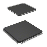
DS72011RB120FPV Renesas Electronics America, DS72011RB120FPV Datasheet - Page 71

DS72011RB120FPV
Manufacturer Part Number
DS72011RB120FPV
Description
IC SH7201 MPU ROMLESS 176LQFP
Manufacturer
Renesas Electronics America
Series
SuperH® SH7200r
Datasheet
1.R0K572011S000BE.pdf
(1222 pages)
Specifications of DS72011RB120FPV
Core Size
32-Bit
Core Processor
SH-2A
Speed
120MHz
Connectivity
CAN, EBI/EMI, FIFO, I²C, SCI, Serial Sound
Peripherals
DMA, POR, PWM, WDT
Number Of I /o
104
Program Memory Type
ROMless
Ram Size
32K x 8
Voltage - Supply (vcc/vdd)
3 V ~ 3.6 V
Data Converters
A/D 8x10b; D/A 2x8b
Oscillator Type
Internal
Operating Temperature
-20°C ~ 70°C
Package / Case
176-LQFP
No. Of I/o's
109
Ram Memory Size
32KB
Cpu Speed
120MHz
Digital Ic Case Style
LQFP
Supply Voltage Range
3V To 3.6V
Operating Temperature Range
-20°C To +70°C
Embedded Interface Type
I2C, SSI
Rohs Compliant
Yes
Lead Free Status / RoHS Status
Lead free / RoHS Compliant
For Use With
R0K572011S000BE - KIT STARTER FOR SH7201HS0005KCU11H - EMULATOR E10A-USB H8S(X),SH2(A)
Eeprom Size
-
Program Memory Size
-
Lead Free Status / RoHS Status
Lead free / RoHS Compliant, Lead free / RoHS Compliant
Available stocks
Company
Part Number
Manufacturer
Quantity
Price
Company:
Part Number:
DS72011RB120FPV
Manufacturer:
Renesas Electronics America
Quantity:
10 000
- Current page: 71 of 1222
- Download datasheet (8Mb)
SH7201 Group
The table below shows the format of instruction codes, operation, and execution states. They are
described by using this format according to their classification.
Notes: 1. Instruction execution cycles: The execution cycles shown in the table are minimums. In
R01UH0026EJ0300 Rev. 3.00
Sep 24, 2010
Instruction
Indicated by mnemonic.
Explanation of Symbols
Rm: Source register
Rn:
imm: Immediate data
disp: Displacement*
Destination register
2. Depending on the operand size, displacement is scaled by ×1, ×2, or ×4. For details,
practice, the number of instruction execution states will be increased in cases such as
the following:
a. When there is a conflict between an instruction fetch and a data access
b. When the destination register of a load instruction (memory → register) is the same
refer to the SH-2A, SH2A-FPU Software Manual.
as the register used by the next instruction.
2
Instruction Code
Indicated in MSB ↔
LSB order.
Explanation of Symbols
mmmm: Source register
nnnn: Destination register
iiii:
dddd:
0000: R0
0001: R1
.........
1111: R15
Immediate data
Displacement
Operation
Indicates summary of
operation.
Explanation of Symbols
→, ←:
(xx):
M/Q/T: Flag bits in SR
&:
|:
^:
~:
<<n: n-bit left shift
>>n: n-bit right shift
Logical AND of each bit
Logical OR of each bit
Exclusive logical OR of
each bit
Logical NOT of each bit
Transfer direction
Memory operand
Execution
States
Value when no
wait states are
inserted. *
1
T Bit
Value of T bit after
instruction is
executed.
Explanation of
Symbols
—: No change
Page 43 of 1190
Section 2 CPU
Related parts for DS72011RB120FPV
Image
Part Number
Description
Manufacturer
Datasheet
Request
R

Part Number:
Description:
KIT STARTER FOR M16C/29
Manufacturer:
Renesas Electronics America
Datasheet:

Part Number:
Description:
KIT STARTER FOR R8C/2D
Manufacturer:
Renesas Electronics America
Datasheet:

Part Number:
Description:
R0K33062P STARTER KIT
Manufacturer:
Renesas Electronics America
Datasheet:

Part Number:
Description:
KIT STARTER FOR R8C/23 E8A
Manufacturer:
Renesas Electronics America
Datasheet:

Part Number:
Description:
KIT STARTER FOR R8C/25
Manufacturer:
Renesas Electronics America
Datasheet:

Part Number:
Description:
KIT STARTER H8S2456 SHARPE DSPLY
Manufacturer:
Renesas Electronics America
Datasheet:

Part Number:
Description:
KIT STARTER FOR R8C38C
Manufacturer:
Renesas Electronics America
Datasheet:

Part Number:
Description:
KIT STARTER FOR R8C35C
Manufacturer:
Renesas Electronics America
Datasheet:

Part Number:
Description:
KIT STARTER FOR R8CL3AC+LCD APPS
Manufacturer:
Renesas Electronics America
Datasheet:

Part Number:
Description:
KIT STARTER FOR RX610
Manufacturer:
Renesas Electronics America
Datasheet:

Part Number:
Description:
KIT STARTER FOR R32C/118
Manufacturer:
Renesas Electronics America
Datasheet:

Part Number:
Description:
KIT DEV RSK-R8C/26-29
Manufacturer:
Renesas Electronics America
Datasheet:

Part Number:
Description:
KIT STARTER FOR SH7124
Manufacturer:
Renesas Electronics America
Datasheet:

Part Number:
Description:
KIT STARTER FOR H8SX/1622
Manufacturer:
Renesas Electronics America
Datasheet:

Part Number:
Description:
KIT DEV FOR SH7203
Manufacturer:
Renesas Electronics America
Datasheet:


