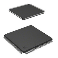
DS72011RB120FPV Renesas Electronics America, DS72011RB120FPV Datasheet - Page 784

DS72011RB120FPV
Manufacturer Part Number
DS72011RB120FPV
Description
IC SH7201 MPU ROMLESS 176LQFP
Manufacturer
Renesas Electronics America
Series
SuperH® SH7200r
Datasheet
1.R0K572011S000BE.pdf
(1222 pages)
Specifications of DS72011RB120FPV
Core Size
32-Bit
Core Processor
SH-2A
Speed
120MHz
Connectivity
CAN, EBI/EMI, FIFO, I²C, SCI, Serial Sound
Peripherals
DMA, POR, PWM, WDT
Number Of I /o
104
Program Memory Type
ROMless
Ram Size
32K x 8
Voltage - Supply (vcc/vdd)
3 V ~ 3.6 V
Data Converters
A/D 8x10b; D/A 2x8b
Oscillator Type
Internal
Operating Temperature
-20°C ~ 70°C
Package / Case
176-LQFP
No. Of I/o's
109
Ram Memory Size
32KB
Cpu Speed
120MHz
Digital Ic Case Style
LQFP
Supply Voltage Range
3V To 3.6V
Operating Temperature Range
-20°C To +70°C
Embedded Interface Type
I2C, SSI
Rohs Compliant
Yes
Lead Free Status / RoHS Status
Lead free / RoHS Compliant
For Use With
R0K572011S000BE - KIT STARTER FOR SH7201HS0005KCU11H - EMULATOR E10A-USB H8S(X),SH2(A)
Eeprom Size
-
Program Memory Size
-
Lead Free Status / RoHS Status
Lead free / RoHS Compliant, Lead free / RoHS Compliant
Available stocks
Company
Part Number
Manufacturer
Quantity
Price
Company:
Part Number:
DS72011RB120FPV
Manufacturer:
Renesas Electronics America
Quantity:
10 000
- Current page: 784 of 1222
- Download datasheet (8Mb)
Section 17 I
17.4.5
In slave receive mode, the master device outputs the transmit clock and transmit data, and the
slave device returns an acknowledge signal. For slave receive mode operation timing, refer to
figures 17.11 and 17.12. The reception procedure and operations in slave receive mode are
described below.
1. Set the ICE bit in ICCR1 to 1. Set bits CKS[3:0] in ICCR1. (Initial setting) Set the MST and
2. When the slave address matches in the first frame following detection of the start condition,
3. Read ICDRR every time RDRF is set. If 8th receive clock pulse falls while RDRF is 1, SCL is
4. The last byte data is read by reading ICDRR.
Page 756 of 1190
(Master output)
(Master output)
(Slave output)
(Slave output)
TRS bits in ICCR1 to select slave receive mode, and wait until the slave address matches.
the slave device outputs the level specified by ACKBT in ICIER to SDA, at the rise of the 9th
clock pulse. At the same time, RDRF in ICSR is set to read ICDRR (dummy read). (Since the
read data show the slave address and R/W, it is not used.)
fixed low until ICDRR is read. The change of the acknowledge before reading ICDRR, to be
returned to the master device, is reflected to the next transmit frame.
processing
ICDRR
ICDRS
RDRF
SCL
SDA
SDA
User
SCL
Slave Receive Operation
2
C Bus Interface 3 (IIC3)
Figure 17.11 Slave Receive Mode Operation Timing (1)
[2] Read ICDRR (dummy read)
A
9
Bit 7
1
Data 1
Bit 6
2
Bit 5
3
Bit 4
4
Bit 3
5
Bit 2
6
Bit 1
7
R01UH0026EJ0300 Rev. 3.00
Bit 0
8
[2] Read ICDRR
A
9
SH7201 Group
Sep 24, 2010
Bit 7
Data 1
1
Data 2
Related parts for DS72011RB120FPV
Image
Part Number
Description
Manufacturer
Datasheet
Request
R

Part Number:
Description:
KIT STARTER FOR M16C/29
Manufacturer:
Renesas Electronics America
Datasheet:

Part Number:
Description:
KIT STARTER FOR R8C/2D
Manufacturer:
Renesas Electronics America
Datasheet:

Part Number:
Description:
R0K33062P STARTER KIT
Manufacturer:
Renesas Electronics America
Datasheet:

Part Number:
Description:
KIT STARTER FOR R8C/23 E8A
Manufacturer:
Renesas Electronics America
Datasheet:

Part Number:
Description:
KIT STARTER FOR R8C/25
Manufacturer:
Renesas Electronics America
Datasheet:

Part Number:
Description:
KIT STARTER H8S2456 SHARPE DSPLY
Manufacturer:
Renesas Electronics America
Datasheet:

Part Number:
Description:
KIT STARTER FOR R8C38C
Manufacturer:
Renesas Electronics America
Datasheet:

Part Number:
Description:
KIT STARTER FOR R8C35C
Manufacturer:
Renesas Electronics America
Datasheet:

Part Number:
Description:
KIT STARTER FOR R8CL3AC+LCD APPS
Manufacturer:
Renesas Electronics America
Datasheet:

Part Number:
Description:
KIT STARTER FOR RX610
Manufacturer:
Renesas Electronics America
Datasheet:

Part Number:
Description:
KIT STARTER FOR R32C/118
Manufacturer:
Renesas Electronics America
Datasheet:

Part Number:
Description:
KIT DEV RSK-R8C/26-29
Manufacturer:
Renesas Electronics America
Datasheet:

Part Number:
Description:
KIT STARTER FOR SH7124
Manufacturer:
Renesas Electronics America
Datasheet:

Part Number:
Description:
KIT STARTER FOR H8SX/1622
Manufacturer:
Renesas Electronics America
Datasheet:

Part Number:
Description:
KIT DEV FOR SH7203
Manufacturer:
Renesas Electronics America
Datasheet:


