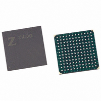
EZ80F91NA050SC Zilog, EZ80F91NA050SC Datasheet - Page 113

EZ80F91NA050SC
Manufacturer Part Number
EZ80F91NA050SC
Description
IC ACCLAIM MCU 256KB 144-BGA
Manufacturer
Zilog
Series
eZ80® Acclaim!®r
Specifications of EZ80F91NA050SC
Core Processor
Z8
Core Size
8-Bit
Speed
50MHz
Connectivity
Ethernet, I²C, IrDA, SPI, UART/USART
Peripherals
Brown-out Detect/Reset, POR, PWM, WDT
Number Of I /o
32
Program Memory Size
256KB (256K x 8)
Program Memory Type
FLASH
Ram Size
16K x 8
Voltage - Supply (vcc/vdd)
3 V ~ 3.6 V
Oscillator Type
Internal
Operating Temperature
0°C ~ 70°C
Package / Case
144-LBGA
Data Bus Width
8 bit
Maximum Clock Frequency
50 MHz
Data Ram Size
16 KB
Number Of Programmable I/os
32
Number Of Timers
16 Bit
Operating Supply Voltage
3 V to 3.6 V
Mounting Style
SMD/SMT
Height
1.5 mm
Length
13 mm
Maximum Operating Temperature
+ 70 C
Minimum Operating Temperature
0 C
Width
13 mm
For Use With
269-4712 - KIT DEV ENCORE 32 SERIES269-4671 - BOARD ZDOTS SBC Z80ACCLAIM PLUS269-4561 - KIT DEV FOR EZ80F91 W/C-COMPILER269-4560 - KIT DEV FOR EZ80F91 W/C-COMPILER
Lead Free Status / RoHS Status
Contains lead / RoHS non-compliant
Eeprom Size
-
Data Converters
-
Lead Free Status / Rohs Status
No RoHS Version Available
Other names
269-3251
Available stocks
Company
Part Number
Manufacturer
Quantity
Price
- Current page: 113 of 384
- Download datasheet (3Mb)
PS019215-0910
Flash Address Upper Byte Register
The FLASH_ADDR_U register defines the upper 6 bits of the Flash memory address
space. Changing the value of FLASH_ADDR_U allows on-chip 256 KB Flash memory
to be mapped to any location within the 16 MB linear address space of the eZ80F91
device. If on-chip Flash memory is enabled, the Flash address assumes priority over any
external Chip Selects. The external Chip Select signals are not asserted if the corre-
sponding Flash address is enabled. Internal Flash memory does not hold priority over
internal SRAM. See
Table 37. Flash Address Upper Byte Register
Bit
Reset
CPU Access
Note: R/W = Read/Write; R = Read Only.
Bit Position
[7:2]
FLASH_ADDR_U
[1:0]
Value
00h–FCh These bits define the upper byte of the Flash address.
00
Table
R/W
37.
7
0
Description
When on-chip Flash is enabled, the Flash address space
begins at address {FLASH_ADDR_U, 00b, 0000h}. On-chip
Flash has priority over all external Chip Selects.
Reserved (enforces alignment on a 256 KB boundary).
R/W
6
0
R/W
5
0
R/W
4
0
(FLASH_ADDR_U = 00F7h)
R/W
3
0
Product Specification
R/W
2
0
eZ80F91 MCU
R
1
0
Flash Memory
R
0
0
104
Related parts for EZ80F91NA050SC
Image
Part Number
Description
Manufacturer
Datasheet
Request
R

Part Number:
Description:
Communication Controllers, ZILOG INTELLIGENT PERIPHERAL CONTROLLER (ZIP)
Manufacturer:
Zilog, Inc.
Datasheet:

Part Number:
Description:
KIT DEV FOR Z8 ENCORE 16K TO 64K
Manufacturer:
Zilog
Datasheet:

Part Number:
Description:
KIT DEV Z8 ENCORE XP 28-PIN
Manufacturer:
Zilog
Datasheet:

Part Number:
Description:
DEV KIT FOR Z8 ENCORE 8K/4K
Manufacturer:
Zilog
Datasheet:

Part Number:
Description:
KIT DEV Z8 ENCORE XP 28-PIN
Manufacturer:
Zilog
Datasheet:

Part Number:
Description:
DEV KIT FOR Z8 ENCORE 4K TO 8K
Manufacturer:
Zilog
Datasheet:

Part Number:
Description:
CMOS Z8 microcontroller. ROM 16 Kbytes, RAM 256 bytes, speed 16 MHz, 32 lines I/O, 3.0V to 5.5V
Manufacturer:
Zilog, Inc.
Datasheet:

Part Number:
Description:
Low-cost microcontroller. 512 bytes ROM, 61 bytes RAM, 8 MHz
Manufacturer:
Zilog, Inc.
Datasheet:

Part Number:
Description:
Z8 4K OTP Microcontroller
Manufacturer:
Zilog, Inc.
Datasheet:

Part Number:
Description:
CMOS SUPER8 ROMLESS MCU
Manufacturer:
Zilog, Inc.
Datasheet:

Part Number:
Description:
SL1866 CMOSZ8 OTP Microcontroller
Manufacturer:
Zilog, Inc.
Datasheet:

Part Number:
Description:
SL1866 CMOSZ8 OTP Microcontroller
Manufacturer:
Zilog, Inc.
Datasheet:

Part Number:
Description:
OTP (KB) = 1, RAM = 125, Speed = 12, I/O = 14, 8-bit Timers = 2, Comm Interfaces Other Features = Por, LV Protect, Voltage = 4.5-5.5V
Manufacturer:
Zilog, Inc.
Datasheet:

Part Number:
Description:
Manufacturer:
Zilog, Inc.
Datasheet:


