EZ80F91NA050SC Zilog, EZ80F91NA050SC Datasheet - Page 65
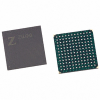
EZ80F91NA050SC
Manufacturer Part Number
EZ80F91NA050SC
Description
IC ACCLAIM MCU 256KB 144-BGA
Manufacturer
Zilog
Series
eZ80® Acclaim!®r
Specifications of EZ80F91NA050SC
Core Processor
Z8
Core Size
8-Bit
Speed
50MHz
Connectivity
Ethernet, I²C, IrDA, SPI, UART/USART
Peripherals
Brown-out Detect/Reset, POR, PWM, WDT
Number Of I /o
32
Program Memory Size
256KB (256K x 8)
Program Memory Type
FLASH
Ram Size
16K x 8
Voltage - Supply (vcc/vdd)
3 V ~ 3.6 V
Oscillator Type
Internal
Operating Temperature
0°C ~ 70°C
Package / Case
144-LBGA
Data Bus Width
8 bit
Maximum Clock Frequency
50 MHz
Data Ram Size
16 KB
Number Of Programmable I/os
32
Number Of Timers
16 Bit
Operating Supply Voltage
3 V to 3.6 V
Mounting Style
SMD/SMT
Height
1.5 mm
Length
13 mm
Maximum Operating Temperature
+ 70 C
Minimum Operating Temperature
0 C
Width
13 mm
For Use With
269-4712 - KIT DEV ENCORE 32 SERIES269-4671 - BOARD ZDOTS SBC Z80ACCLAIM PLUS269-4561 - KIT DEV FOR EZ80F91 W/C-COMPILER269-4560 - KIT DEV FOR EZ80F91 W/C-COMPILER
Lead Free Status / RoHS Status
Contains lead / RoHS non-compliant
Eeprom Size
-
Data Converters
-
Lead Free Status / Rohs Status
No RoHS Version Available
Other names
269-3251
Available stocks
Company
Part Number
Manufacturer
Quantity
Price


Table 9. Port x Alternate Registers 0
(PA_ALT0 = 00A6h, PB_ALT0 = 00A7h, PC_ALT0 = 00CEh, PD_ALT0 = 00CFh)
Table 10. Port x Alternate Registers 1
(PA_ALT1 = 0098h, PB_ALT1 = 009Ch, PC_ALT1 = 00A0h, PD_ALT1 = 00A4h)
Table 11. Port x Alternate Registers 2
(PA_ALT2 = 0099h, PB_ALT2 = 009Dh, PC_ALT2 = 00A1h, PD_ALT2 = 00A5h)
PS019215-0910
Bit
Reset
CPU Access
Note: W = Write only
Bit
Reset
CPU Access
Note: R/W = Read/Write.
Bit
Reset
CPU Access
Note: R/W = Read/Write.
Port x Alternate Register 0
The Port x Alternate register 0 is used to clear edge triggered interrupts. If an edge
triggered interrupt occurs, writing 1 to the corresponding bit of this register will clear it.
Port x Alternate Register 1
In conjunction with the other GPIO Control registers, the Port x Alternate Register 1 (see
Table
mode selection, see
Port x Alternate Register 2
In conjunction with the other GPIO Control registers, the Port x Alternate Register 2 (see
Table
mode selection, see
10) controls the operating modes of the GPIO port pins. For more details on GPIO
11) controls the operating modes of the GPIO port pins. For more details on GPIO
R/W
R/W
W
7
0
7
0
7
0
R/W
R/W
W
6
0
6
0
6
0
Table 6
Table 6
R/W
R/W
W
5
0
5
0
5
0
on page 50.
on page 50.
R/W
R/W
W
4
0
4
0
4
0
R/W
R/W
W
3
0
3
0
3
0
R/W
R/W
W
2
0
2
0
2
0
R/W
R/W
W
1
0
1
0
1
0
General-Purpose Input/Output
Product Specification
R/W
R/W
W
0
0
0
0
0
0
eZ80F91 MCU
56
Related parts for EZ80F91NA050SC
Image
Part Number
Description
Manufacturer
Datasheet
Request
R

Part Number:
Description:
Communication Controllers, ZILOG INTELLIGENT PERIPHERAL CONTROLLER (ZIP)
Manufacturer:
Zilog, Inc.
Datasheet:

Part Number:
Description:
KIT DEV FOR Z8 ENCORE 16K TO 64K
Manufacturer:
Zilog
Datasheet:

Part Number:
Description:
KIT DEV Z8 ENCORE XP 28-PIN
Manufacturer:
Zilog
Datasheet:

Part Number:
Description:
DEV KIT FOR Z8 ENCORE 8K/4K
Manufacturer:
Zilog
Datasheet:

Part Number:
Description:
KIT DEV Z8 ENCORE XP 28-PIN
Manufacturer:
Zilog
Datasheet:

Part Number:
Description:
DEV KIT FOR Z8 ENCORE 4K TO 8K
Manufacturer:
Zilog
Datasheet:
Part Number:
Description:
CMOS Z8 microcontroller. ROM 16 Kbytes, RAM 256 bytes, speed 16 MHz, 32 lines I/O, 3.0V to 5.5V
Manufacturer:
Zilog, Inc.
Datasheet:
Part Number:
Description:
Low-cost microcontroller. 512 bytes ROM, 61 bytes RAM, 8 MHz
Manufacturer:
Zilog, Inc.
Datasheet:
Part Number:
Description:
Z8 4K OTP Microcontroller
Manufacturer:
Zilog, Inc.
Datasheet:
Part Number:
Description:
CMOS SUPER8 ROMLESS MCU
Manufacturer:
Zilog, Inc.
Datasheet:
Part Number:
Description:
SL1866 CMOSZ8 OTP Microcontroller
Manufacturer:
Zilog, Inc.
Datasheet:
Part Number:
Description:
SL1866 CMOSZ8 OTP Microcontroller
Manufacturer:
Zilog, Inc.
Datasheet:
Part Number:
Description:
OTP (KB) = 1, RAM = 125, Speed = 12, I/O = 14, 8-bit Timers = 2, Comm Interfaces Other Features = Por, LV Protect, Voltage = 4.5-5.5V
Manufacturer:
Zilog, Inc.
Datasheet:
Part Number:
Description:
Manufacturer:
Zilog, Inc.
Datasheet: