EZ80F91NA050SC Zilog, EZ80F91NA050SC Datasheet - Page 269
EZ80F91NA050SC
Manufacturer Part Number
EZ80F91NA050SC
Description
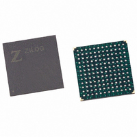
IC ACCLAIM MCU 256KB 144-BGA
Manufacturer
Zilog
Series
eZ80® Acclaim!®r
Specifications of EZ80F91NA050SC
Core Processor
Z8
Core Size
8-Bit
Speed
50MHz
Connectivity
Ethernet, I²C, IrDA, SPI, UART/USART
Peripherals
Brown-out Detect/Reset, POR, PWM, WDT
Number Of I /o
32
Program Memory Size
256KB (256K x 8)
Program Memory Type
FLASH
Ram Size
16K x 8
Voltage - Supply (vcc/vdd)
3 V ~ 3.6 V
Oscillator Type
Internal
Operating Temperature
0°C ~ 70°C
Package / Case
144-LBGA
Data Bus Width
8 bit
Maximum Clock Frequency
50 MHz
Data Ram Size
16 KB
Number Of Programmable I/os
32
Number Of Timers
16 Bit
Operating Supply Voltage
3 V to 3.6 V
Mounting Style
SMD/SMT
Height
1.5 mm
Length
13 mm
Maximum Operating Temperature
+ 70 C
Minimum Operating Temperature
0 C
Width
13 mm
For Use With
269-4712 - KIT DEV ENCORE 32 SERIES269-4671 - BOARD ZDOTS SBC Z80ACCLAIM PLUS269-4561 - KIT DEV FOR EZ80F91 W/C-COMPILER269-4560 - KIT DEV FOR EZ80F91 W/C-COMPILER
Lead Free Status / RoHS Status
Contains lead / RoHS non-compliant
Eeprom Size
-
Data Converters
-
Lead Free Status / Rohs Status
No RoHS Version Available
Other names
269-3251
Available stocks
Company
Part Number
Manufacturer
Quantity
Price


Table 151. Pin to Boundary Scan Cell Mapping
PS019215-0910
Pin
TRIGOUT
TRIGOUT
TRIGOUT
HALT_SLP
BUSACK
BUSREQ
NMI
RESET
RESET_OUT
WAIT
INSTRD
WR
WR
RD
MREQ
Boundary Scan Cell Functionality
The boundary scan cells implemented are analogous to cell BC_1, defined in the Standard
VHDL Package STD_1149_1_2001.
All boundary scan cells are of the type control-and-observe; they provide both controlla-
bility and observability for the pins to which they are connected. For open-drain outputs
and bidirectional pins, this type includes controllability and observability of output
enables.
Chain Sequence and Length
When enabled to shift data, the boundary scan shift register is connected to TDI at the
input line for TRIGOUT and to TDO at PD0. The shift register is arranged so that data is
shifted via the pins starting to the left of the OCI interface pins and proceeding clockwise
around the chip. If a pin features multiple scannable bits (example: bidirectional pins or
open-drain output pins), the data is shifted first into the input signal, then the output, then
the output enable (OEN).
The boundary scan register is 213 bits wide.
register, numbering them in clockwise order.
Direction
Output
Output
Output
Output
Output
Output
Output
Input
Input
Input
Input
Input
Input
OEN
OEN
Scan Cell No
10
12
13
14
11
0
1
2
3
4
5
6
7
8
9
Pin
MII_TxD2
MII_TxD3
MII_COL
MII_CRS
PA7
PA7
PA7
PA6
PA6
PA6
PA5
PA5
PA5
PA4
PA4
Table 151
lists the ordering of bits in the shift
Direction
Output
Output
Output
Output
Output
Output
Product Specification
Input
Input
Input
Input
Input
Input
OEN
OEN
OEN
On-Chip Instrumentation
eZ80F91 MCU
Scan Cell No
107
109
120
121
108
110
112
113
114
115
116
117
118
119
111
260
Related parts for EZ80F91NA050SC
Image
Part Number
Description
Manufacturer
Datasheet
Request
R

Part Number:
Description:
Communication Controllers, ZILOG INTELLIGENT PERIPHERAL CONTROLLER (ZIP)
Manufacturer:
Zilog, Inc.
Datasheet:

Part Number:
Description:
KIT DEV FOR Z8 ENCORE 16K TO 64K
Manufacturer:
Zilog
Datasheet:

Part Number:
Description:
KIT DEV Z8 ENCORE XP 28-PIN
Manufacturer:
Zilog
Datasheet:

Part Number:
Description:
DEV KIT FOR Z8 ENCORE 8K/4K
Manufacturer:
Zilog
Datasheet:

Part Number:
Description:
KIT DEV Z8 ENCORE XP 28-PIN
Manufacturer:
Zilog
Datasheet:

Part Number:
Description:
DEV KIT FOR Z8 ENCORE 4K TO 8K
Manufacturer:
Zilog
Datasheet:
Part Number:
Description:
CMOS Z8 microcontroller. ROM 16 Kbytes, RAM 256 bytes, speed 16 MHz, 32 lines I/O, 3.0V to 5.5V
Manufacturer:
Zilog, Inc.
Datasheet:
Part Number:
Description:
Low-cost microcontroller. 512 bytes ROM, 61 bytes RAM, 8 MHz
Manufacturer:
Zilog, Inc.
Datasheet:
Part Number:
Description:
Z8 4K OTP Microcontroller
Manufacturer:
Zilog, Inc.
Datasheet:
Part Number:
Description:
CMOS SUPER8 ROMLESS MCU
Manufacturer:
Zilog, Inc.
Datasheet:
Part Number:
Description:
SL1866 CMOSZ8 OTP Microcontroller
Manufacturer:
Zilog, Inc.
Datasheet:
Part Number:
Description:
SL1866 CMOSZ8 OTP Microcontroller
Manufacturer:
Zilog, Inc.
Datasheet:
Part Number:
Description:
OTP (KB) = 1, RAM = 125, Speed = 12, I/O = 14, 8-bit Timers = 2, Comm Interfaces Other Features = Por, LV Protect, Voltage = 4.5-5.5V
Manufacturer:
Zilog, Inc.
Datasheet:
Part Number:
Description:
Manufacturer:
Zilog, Inc.
Datasheet: