PIC18F45K80-I/PT Microchip Technology, PIC18F45K80-I/PT Datasheet - Page 437
PIC18F45K80-I/PT
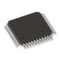
Manufacturer Part Number
PIC18F45K80-I/PT
Description
MCU PIC 32KB FLASH 44TQFP
Manufacturer
Microchip Technology
Series
PIC® XLP™ 18Fr
Datasheet
1.PIC18F25K80-ISO.pdf
(628 pages)
Specifications of PIC18F45K80-I/PT
Core Size
8-Bit
Program Memory Size
32KB (16K x 16)
Peripherals
Brown-out Detect/Reset, LVD, POR, PWM, WDT
Core Processor
PIC
Speed
64MHz
Connectivity
ECAN, I²C, LIN, SPI, UART/USART
Number Of I /o
35
Program Memory Type
FLASH
Eeprom Size
1K x 8
Ram Size
3.6K x 8
Voltage - Supply (vcc/vdd)
1.8 V ~ 5.5 V
Data Converters
A/D 11x12b
Oscillator Type
Internal
Operating Temperature
-40°C ~ 85°C
Package / Case
44-TQFP
Controller Family/series
PIC18
Ram Memory Size
4KB
Cpu Speed
16MIPS
No. Of Pwm Channels
5
Embedded Interface Type
I2C, SPI, USART
Processor Series
PIC18F45K80
Core
PIC
Data Bus Width
8 bit
Data Ram Size
1 KB
Interface Type
I2C, SPI, USART
Maximum Clock Frequency
64 MHz
Number Of Programmable I/os
35
Number Of Timers
5
Operating Supply Voltage
1.8 V to 5.5 V
Maximum Operating Temperature
+ 85 C
Mounting Style
SMD/SMT
Lead Free Status / RoHS Status
Lead free / RoHS Compliant
Lead Free Status / RoHS Status
Lead free / RoHS Compliant
Available stocks
Company
Part Number
Manufacturer
Quantity
Price
Company:

Part Number:
PIC18F45K80-I/PT
Manufacturer:
MICROCHIP
Quantity:
1 500
Company:
Part Number:
PIC18F45K80-I/PT
Manufacturer:
PIC
Quantity:
400
Company:
Part Number:
PIC18F45K80-I/PT
Manufacturer:
Microchip Technology
Quantity:
10 000
Part Number:
PIC18F45K80-I/PT
Manufacturer:
MICROCHIP/微芯
Quantity:
20 000


27.2.5
This register controls the operation of the CAN module’s
I/O pins in relation to the rest of the microcontroller.
REGISTER 27-55: CIOCON: CAN I/O CONTROL REGISTER
2011 Microchip Technology Inc.
bit 7
Legend:
R = Readable bit
-n = Value at POR
bit 7
bit 6
bit 5
bit 4
bit 3-1
bit 0
Note 1:
TX2SRC
R/W-0
Always set this bit when using a differential bus to avoid signal crosstalk in CANTX from other nearby pins.
CAN MODULE I/O CONTROL
REGISTER
TX2SRC: CANTX2 Pin Data Source bit
1 = CANTX2 pin will output the CAN clock
0 = CANTX2 pin will output CANTX
TX2EN: CANTX Pin Enable bit
1 = CANTX2 pin will output CANTX or CAN clock as selected by the TX2SRC bit
0 = CANTX2 pin will have digital I/O function
ENDRHI: Enable Drive High bit
1 = CANTX pin will drive V
0 = CANTX pin will be tri-state when recessive
CANCAP: CAN Message Receive Capture Enable bit
1 = Enable CAN capture; CAN message receive signal replaces input on RC2/CCP1
0 = Disable CAN capture; RC2/CCP1 input to CCP1 module
Unimplemented: Read as ‘ 0 ’
CLKSEL: CAN Clock Source Selection bit
1 = Use the oscillator as the source of the CAN system clock
0 = Use the PLL as the source of the CAN system clock
TX2EN
R/W-0
W = Writable bit
‘1’ = Bit is set
ENDRHI
R/W-0
(1)
DD
when recessive
CANCAP
(1)
R/W-0
Preliminary
U = Unimplemented bit, read as ‘0’
‘0’ = Bit is cleared
PIC18F66K80 FAMILY
U-0
—
U-0
—
x = Bit is unknown
U-0
—
DS39977C-page 437
CLKSEL
R/W-0
bit 0
Related parts for PIC18F45K80-I/PT
Image
Part Number
Description
Manufacturer
Datasheet
Request
R

Part Number:
Description:
Manufacturer:
Microchip Technology Inc.
Datasheet:
Part Number:
Description:
Manufacturer:
Microchip Technology Inc.
Datasheet:
Part Number:
Description:
Manufacturer:
Microchip Technology Inc.
Datasheet:
Part Number:
Description:
Manufacturer:
Microchip Technology Inc.
Datasheet:
Part Number:
Description:
Manufacturer:
Microchip Technology Inc.
Datasheet:
Part Number:
Description:
Manufacturer:
Microchip Technology Inc.
Datasheet:
Part Number:
Description:
Manufacturer:
Microchip Technology Inc.
Datasheet:
Part Number:
Description:
Manufacturer:
Microchip Technology Inc.
Datasheet: