PIC18F45K80-I/PT Microchip Technology, PIC18F45K80-I/PT Datasheet - Page 477
PIC18F45K80-I/PT
Manufacturer Part Number
PIC18F45K80-I/PT
Description
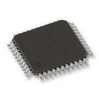
MCU PIC 32KB FLASH 44TQFP
Manufacturer
Microchip Technology
Series
PIC® XLP™ 18Fr
Datasheet
1.PIC18F25K80-ISO.pdf
(628 pages)
Specifications of PIC18F45K80-I/PT
Core Size
8-Bit
Program Memory Size
32KB (16K x 16)
Peripherals
Brown-out Detect/Reset, LVD, POR, PWM, WDT
Core Processor
PIC
Speed
64MHz
Connectivity
ECAN, I²C, LIN, SPI, UART/USART
Number Of I /o
35
Program Memory Type
FLASH
Eeprom Size
1K x 8
Ram Size
3.6K x 8
Voltage - Supply (vcc/vdd)
1.8 V ~ 5.5 V
Data Converters
A/D 11x12b
Oscillator Type
Internal
Operating Temperature
-40°C ~ 85°C
Package / Case
44-TQFP
Controller Family/series
PIC18
Ram Memory Size
4KB
Cpu Speed
16MIPS
No. Of Pwm Channels
5
Embedded Interface Type
I2C, SPI, USART
Processor Series
PIC18F45K80
Core
PIC
Data Bus Width
8 bit
Data Ram Size
1 KB
Interface Type
I2C, SPI, USART
Maximum Clock Frequency
64 MHz
Number Of Programmable I/os
35
Number Of Timers
5
Operating Supply Voltage
1.8 V to 5.5 V
Maximum Operating Temperature
+ 85 C
Mounting Style
SMD/SMT
Lead Free Status / RoHS Status
Lead free / RoHS Compliant
Lead Free Status / RoHS Status
Lead free / RoHS Compliant
Available stocks
Company
Part Number
Manufacturer
Quantity
Price
Company:

Part Number:
PIC18F45K80-I/PT
Manufacturer:
MICROCHIP
Quantity:
1 500
Company:
Part Number:
PIC18F45K80-I/PT
Manufacturer:
PIC
Quantity:
400
Company:
Part Number:
PIC18F45K80-I/PT
Manufacturer:
Microchip Technology
Quantity:
10 000
Part Number:
PIC18F45K80-I/PT
Manufacturer:
MICROCHIP/微芯
Quantity:
20 000


28.2.1
Register 28-15
readable and writable register which contains a control
bit that allows software to override the WDT Enable
Configuration bit, but only if the Configuration bit has
disabled the WDT.
REGISTER 28-15: WDTCON: WATCHDOG TIMER CONTROL REGISTER
TABLE 28-2:
2011 Microchip Technology Inc.
bit 7
Legend:
R = Readable bit
-n = Value at POR
bit 7
bit 6
bit 5
bit 4
bit 3
bit 2
bit 1
bit 0
Note 1:
RCON
WDTCON
Legend: — = unimplemented, read as ‘ 0 ’. Shaded cells are not used by the Watchdog Timer.
REGSLP
Name
R/W-0
2:
3:
(3)
This bit has no effect if the Configuration bits, WDTEN<1:0>, are enabled.
This bit is available only when RETEN = 0 .
This bit is disabled on PIC18LF devices.
CONTROL REGISTER
shows the WDTCON register. This is a
REGSLP: Regulator Voltage Sleep Enable bit
1 = Regulator goes into Low-Power mode when device’s Sleep mode is enabled
0 = Regulator stays in normal mode when device’s Sleep mode is activated
Unimplemented : Read as ‘ 0 ’
ULPLVL: Ultra Low-Power Wake-up Output bit
Not valid unless ULPEN = 1 .
1 = Voltage on RA0 pin > ~ 0.5V
0 = Voltage on RA0 pin < ~ 0.5V.
SRETEN: Regulator Voltage Sleep Disable bit
1 = If RETEN (CONFIG1L<0>) = 0 and the regulator is enabled, the device goes into Ultra Low-Power
0 = The regulator is on when device’s Sleep mode is enabled and the Low-Power mode is controlled
Unimplemented : Read as ‘ 0 ’
ULPEN: Ultra Low-Power Wake-up Module Enable bit
1 = Ultra low-power wake-up module is enabled; ULPLVL bit indicates comparator output
0 = Ultra low-power wake-up module is disabled
ULPSINK: Ultra Low-Power Wake-up Current Sink Enable bit
Not valid unless ULPEN = 1 .
1 = Ultra low-power wake-up current sink is enabled
0 = Ultra low-power wake-up current sink is disabled
SWDTEN: Software Controlled Watchdog Timer Enable bit
1 = Watchdog Timer is on
0 = Watchdog Timer is off
REGSLP
SUMMARY OF WATCHDOG TIMER REGISTERS
IPEN
Bit 7
mode in Sleep
by REGSLP
U-0
—
SBOREN
W = Writable bit
‘1’ = Bit is set
Bit 6
—
ULPLVL
R-x
ULPLVL
Bit 5
CM
SRETEN
R/W-0
Preliminary
SRETEN
(2)
Bit 4
RI
U = Unimplemented bit, read as ‘0’
‘0’ = Bit is cleared
PIC18F66K80 FAMILY
(3)
(2)
U-0
—
Bit 3
TO
—
(1)
ULPEN
R/W-x
ULPEN
Bit 2
PD
x = Bit is unknown
ULPSINK
R/W-x
ULPSINK
Bit 1
POR
DS39977C-page 477
SWDTEN
SWDTEN
R/W-0
Bit 0
BOR
bit 0
(1)
Related parts for PIC18F45K80-I/PT
Image
Part Number
Description
Manufacturer
Datasheet
Request
R

Part Number:
Description:
Manufacturer:
Microchip Technology Inc.
Datasheet:
Part Number:
Description:
Manufacturer:
Microchip Technology Inc.
Datasheet:
Part Number:
Description:
Manufacturer:
Microchip Technology Inc.
Datasheet:
Part Number:
Description:
Manufacturer:
Microchip Technology Inc.
Datasheet:
Part Number:
Description:
Manufacturer:
Microchip Technology Inc.
Datasheet:
Part Number:
Description:
Manufacturer:
Microchip Technology Inc.
Datasheet:
Part Number:
Description:
Manufacturer:
Microchip Technology Inc.
Datasheet:
Part Number:
Description:
Manufacturer:
Microchip Technology Inc.
Datasheet: