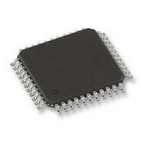
PIC18F45K80-I/PT Microchip Technology, PIC18F45K80-I/PT Datasheet - Page 484

PIC18F45K80-I/PT
Manufacturer Part Number
PIC18F45K80-I/PT
Description
MCU PIC 32KB FLASH 44TQFP
Manufacturer
Microchip Technology
Series
PIC® XLP™ 18Fr
Datasheet
1.PIC18F25K80-ISO.pdf
(628 pages)
Specifications of PIC18F45K80-I/PT
Core Size
8-Bit
Program Memory Size
32KB (16K x 16)
Peripherals
Brown-out Detect/Reset, LVD, POR, PWM, WDT
Core Processor
PIC
Speed
64MHz
Connectivity
ECAN, I²C, LIN, SPI, UART/USART
Number Of I /o
35
Program Memory Type
FLASH
Eeprom Size
1K x 8
Ram Size
3.6K x 8
Voltage - Supply (vcc/vdd)
1.8 V ~ 5.5 V
Data Converters
A/D 11x12b
Oscillator Type
Internal
Operating Temperature
-40°C ~ 85°C
Package / Case
44-TQFP
Controller Family/series
PIC18
Ram Memory Size
4KB
Cpu Speed
16MIPS
No. Of Pwm Channels
5
Embedded Interface Type
I2C, SPI, USART
Processor Series
PIC18F45K80
Core
PIC
Data Bus Width
8 bit
Data Ram Size
1 KB
Interface Type
I2C, SPI, USART
Maximum Clock Frequency
64 MHz
Number Of Programmable I/os
35
Number Of Timers
5
Operating Supply Voltage
1.8 V to 5.5 V
Maximum Operating Temperature
+ 85 C
Mounting Style
SMD/SMT
Lead Free Status / RoHS Status
Lead free / RoHS Compliant
Lead Free Status / RoHS Status
Lead free / RoHS Compliant
Available stocks
Company
Part Number
Manufacturer
Quantity
Price
Company:
Part Number:
PIC18F45K80-I/PT
Manufacturer:
MICROCHIP
Quantity:
1 500
Company:
Part Number:
PIC18F45K80-I/PT
Manufacturer:
PIC
Quantity:
400
Company:
Part Number:
PIC18F45K80-I/PT
Manufacturer:
Microchip Technology
Quantity:
10 000
Part Number:
PIC18F45K80-I/PT
Manufacturer:
MICROCHIP/微芯
Quantity:
20 000
- Current page: 484 of 628
- Download datasheet (6Mb)
PIC18F66K80 FAMILY
TABLE 28-4:
28.6.1
The program memory may be read to, or written from,
any location using the table read and table write
instructions. The Device ID may be read with table
reads. The Configuration registers may be read and
written with the table read and table write instructions.
In normal execution mode, the CPx bits have no direct
effect. CPx bits inhibit external reads and writes. A block
of user memory may be protected from table writes if the
WRTx Configuration bit is ‘ 0 ’.
The EBTRx bits control table reads. For a block of user
memory with the EBTRx bit set to ‘ 0 ’, a table read
instruction that executes from within that block is allowed
to read. A table read instruction that executes from a
FIGURE 28-7:
DS39977C-page 484
300008h CONFIG5L
300009h CONFIG5H
30000Ah CONFIG6L
30000Bh CONFIG6H
30000Ch CONFIG7L
30000Dh CONFIG7H
Legend: Shaded cells are unimplemented.
File Name
TBLPTR = 0008FFh
Results: All table writes are disabled to Blockn whenever WRTx = 0
Register Values
PROGRAM MEMORY
CODE PROTECTION
PC = 00BFFEh
PC = 003FFEh
SUMMARY OF CODE PROTECTION REGISTERS
TABLE WRITE (WRTx) DISALLOWED
WRTD
Bit 7
CPD
—
—
—
—
EBTRB
WRTB
Bit 6
CPB
—
—
—
Program Memory
WRTC
Bit 5
Preliminary
—
—
—
—
—
TBLWT*
TBLWT*
Bit 4
—
—
—
—
—
—
illustrate table write and table read protection.
location outside of that block is not allowed to read and
will result in reading ‘ 0 ’s. Figures
Note:
000000h
0007FFh
000800h
003FFFh
004000h
007FFFh
008000h
00BFFFh
00C000h
00FFFFh
EBTR3
WRT3
Bit 3
CP3
—
—
—
.
Code protection bits may only be written
to a ‘ 0 ’ from a ‘ 1 ’ state. It is not possible to
write a ‘ 1 ’ to a bit in the ‘ 0 ’ state. Code
protection bits are only set to ‘ 1 ’ by a full
chip erase or block erase function. The full
chip erase and block erase functions can
only be initiated via ICSP or an external
programmer.
programming
information.
Configuration Bit Settings
EBTR2
WRT2
Bit 2
CP2
WRTB, EBTRB = 11
WRT0, EBTR0 = 01
WRT1, EBTR1 = 11
WRT2, EBTR2 = 11
WRT3, EBTR3 = 11
—
—
—
2011 Microchip Technology Inc.
Refer
specification
EBTR1
WRT1
Bit 1
CP1
—
—
—
28-7
to
the
through
for
EBTR0
WRT0
Bit 0
CP0
device
—
—
—
more
28-9
Related parts for PIC18F45K80-I/PT
Image
Part Number
Description
Manufacturer
Datasheet
Request
R

Part Number:
Description:
Manufacturer:
Microchip Technology Inc.
Datasheet:

Part Number:
Description:
Manufacturer:
Microchip Technology Inc.
Datasheet:

Part Number:
Description:
Manufacturer:
Microchip Technology Inc.
Datasheet:

Part Number:
Description:
Manufacturer:
Microchip Technology Inc.
Datasheet:

Part Number:
Description:
Manufacturer:
Microchip Technology Inc.
Datasheet:

Part Number:
Description:
Manufacturer:
Microchip Technology Inc.
Datasheet:

Part Number:
Description:
Manufacturer:
Microchip Technology Inc.
Datasheet:

Part Number:
Description:
Manufacturer:
Microchip Technology Inc.
Datasheet:


