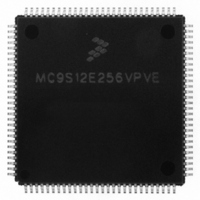
MC9S12E256VPVE Freescale Semiconductor, MC9S12E256VPVE Datasheet - Page 102

MC9S12E256VPVE
Manufacturer Part Number
MC9S12E256VPVE
Description
IC MCU 256K FLASH 25MHZ 112-LQFP
Manufacturer
Freescale Semiconductor
Series
HCS12r
Datasheet
1.MC9S12E256CFUE.pdf
(602 pages)
Specifications of MC9S12E256VPVE
Core Processor
HCS12
Core Size
16-Bit
Speed
25MHz
Connectivity
EBI/EMI, I²C, SCI, SPI
Peripherals
POR, PWM, WDT
Number Of I /o
91
Program Memory Size
256KB (256K x 8)
Program Memory Type
FLASH
Ram Size
16K x 8
Voltage - Supply (vcc/vdd)
2.35 V ~ 2.75 V
Data Converters
A/D 16x10b; D/A 2x8b
Oscillator Type
Internal
Operating Temperature
-40°C ~ 105°C
Package / Case
112-LQFP
Processor Series
S12E
Core
HCS12
Data Bus Width
16 bit
Data Ram Size
16 KB
Interface Type
I2C/SCI/SPI
Maximum Clock Frequency
50 MHz
Number Of Programmable I/os
92
Number Of Timers
12
Maximum Operating Temperature
+ 105 C
Mounting Style
SMD/SMT
3rd Party Development Tools
EWHCS12
Minimum Operating Temperature
- 40 C
On-chip Adc
16-ch x 10-bit
On-chip Dac
2-ch x 8-bit
For Use With
M68EVB912E128 - BOARD EVAL FOR MC9S12E128/64
Lead Free Status / RoHS Status
Lead free / RoHS Compliant
Eeprom Size
-
Lead Free Status / Rohs Status
Lead free / RoHS Compliant
Available stocks
Company
Part Number
Manufacturer
Quantity
Price
Company:
Part Number:
MC9S12E256VPVE
Manufacturer:
Freescale Semiconductor
Quantity:
10 000
- Current page: 102 of 602
- Download datasheet (4Mb)
Chapter 2 256 Kbyte Flash Module (FTS256K2V1)
2.4.1.1
Prior to issuing any program, erase, erase verify, or data compress command, it is first necessary to write
the FCLKDIV register to divide the oscillator clock down to within the 150 kHz to 200 kHz range. Because
the program and erase timings are also a function of the bus clock, the FCLKDIV determination must take
this information into account.
If we define:
Then, FCLKDIV register bits PRDIV8 and FDIV[5:0] are to be set as described in
For example, if the oscillator clock frequency is 950 kHz and the bus clock frequency is 10 MHz,
FCLKDIV bits FDIV[5:0] must be set to 4 (000100) and bit PRDIV8 set to 0. The resulting FCLK
frequency is then 190 kHz. As a result, the Flash program and erase algorithm timings are increased over
the optimum target by:
If the FCLKDIV register is written, the FDIVLD bit is set automatically. If the FDIVLD bit is 0, the
FCLKDIV register has not been written since the last reset. Flash commands will not be executed if the
FCLKDIV register has not been written to.
102
•
•
•
FCLK as the clock of the Flash timing control block,
Tbus as the period of the bus clock, and
INT(x) as taking the integer part of x (e.g. INT(4.323)=4).
Writing the FCLKDIV Register
Program and erase command execution time will increase proportionally
with the period of FCLK. Because of the impact of clock synchronization
on the accuracy of the functional timings, programming or erasing the Flash
memory cannot be performed if the bus clock runs at less than 1 MHz.
Programming or erasing the Flash memory with FCLK < 150 kHz must be
avoided. Setting FCLKDIV to a value such that FCLK < 150 kHz can
destroy the Flash memory due to overstress. Setting FCLKDIV to a value
such that (1/FCLK + Tbus) < 5 s can result in incomplete programming or
erasure of the Flash memory cells.
MC9S12E256 Data Sheet, Rev. 1.08
200 190
–
CAUTION
200 100
=
5%
Figure
Freescale Semiconductor
2-22.
Related parts for MC9S12E256VPVE
Image
Part Number
Description
Manufacturer
Datasheet
Request
R
Part Number:
Description:
Manufacturer:
Freescale Semiconductor, Inc
Datasheet:
Part Number:
Description:
Manufacturer:
Freescale Semiconductor, Inc
Datasheet:
Part Number:
Description:
Manufacturer:
Freescale Semiconductor, Inc
Datasheet:
Part Number:
Description:
Manufacturer:
Freescale Semiconductor, Inc
Datasheet:
Part Number:
Description:
Manufacturer:
Freescale Semiconductor, Inc
Datasheet:
Part Number:
Description:
Manufacturer:
Freescale Semiconductor, Inc
Datasheet:
Part Number:
Description:
Manufacturer:
Freescale Semiconductor, Inc
Datasheet:
Part Number:
Description:
Manufacturer:
Freescale Semiconductor, Inc
Datasheet:
Part Number:
Description:
Manufacturer:
Freescale Semiconductor, Inc
Datasheet:
Part Number:
Description:
Manufacturer:
Freescale Semiconductor, Inc
Datasheet:
Part Number:
Description:
Manufacturer:
Freescale Semiconductor, Inc
Datasheet:
Part Number:
Description:
Manufacturer:
Freescale Semiconductor, Inc
Datasheet:
Part Number:
Description:
Manufacturer:
Freescale Semiconductor, Inc
Datasheet:
Part Number:
Description:
Manufacturer:
Freescale Semiconductor, Inc
Datasheet:
Part Number:
Description:
Manufacturer:
Freescale Semiconductor, Inc
Datasheet:


